


CHAPTER 4 CAUTIONS
User’s Manual U14337EJ1V0UM00
28
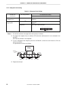
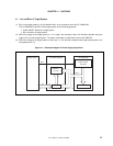
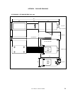
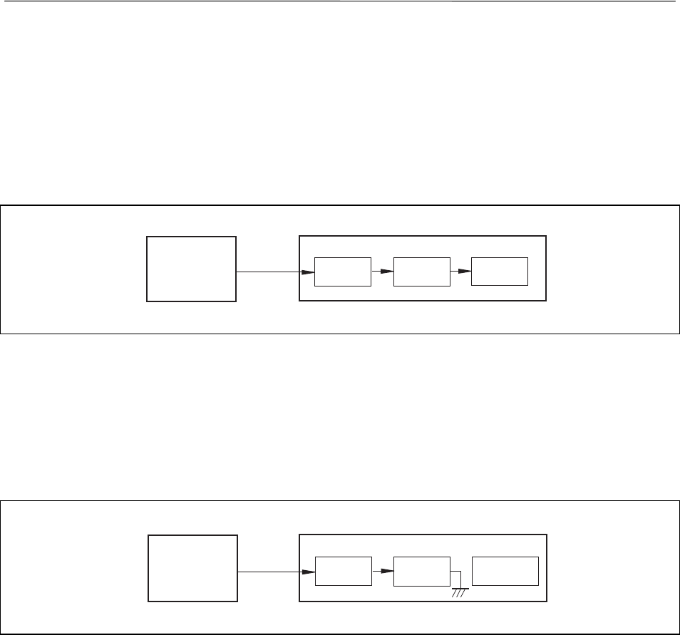
4.2 NMI Signal
The input signal (NMI signal) from the target system is delayed (t
pD
= 0.25 ns (TYP.)) because it passes through
QS3125 (Q switch) before it is input to the I/O chip of the emulator.
In addition, the DC characteristics change. The input voltage becomes V
IH
= 2.0 V (MIN.), V
IL
= 0.8 V (MAX.), and
the input current becomes I
IN
=
±
0.5
µ
A (MAX.).
Figure 4-2. NMI Signal Flow Path
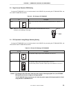
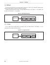
4.3 V
PP
Signal
The V
PP
signal from the target system is connected to LED via a 330-
Ω
resistor in the emulator. It is not
connected to the evaluation chip in the emulator.
Figure 4-3. V
PP
Signal Flow Path
IE-703040-MC-EM1
NMI pin
Target system
NMI signal
QS3125
I/O chip
IE-703040-MC-EM1
330 Ω
Target system
V
PP
signal
LED
Evaluation
chip