


µ
PD75P308
12
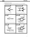
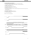
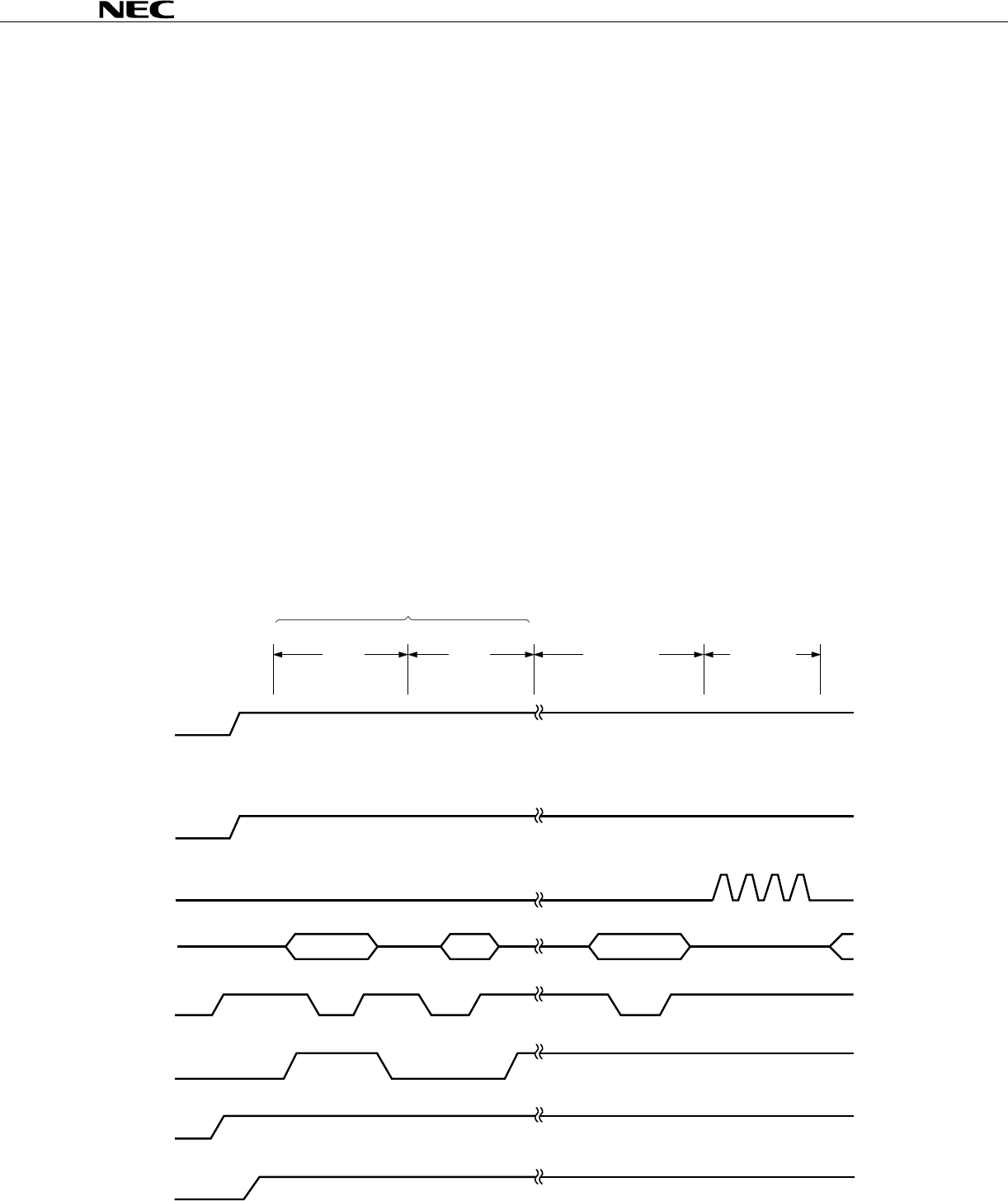
3.2 PROGRAM MEMORY WRITE PROCEDURE
The program memory write procedure is as follows. High-speed program memory write is possible.
(1) Ground the unused pins through pull-down resistors. The X1 pin must be low.
(2) Supply 5 V to the V
DD and VPP pins.
(3) Wait for 10 microseconds.
(4) Set program memory address 0 clear mode.
(5) Supply 6 V to the V
DD pin and 12.5 V to the VPP pin.
(6) Set program inhibit mode.
(7) Write data in 1-millisecond write mode.
(8) Set program inhibit mode.
(9) Set verify mode. If data has been written connectly, proceed to step (10). If data has not yet been
written, repeat steps (7) to (9).
(10) Write additional data for (the number of times data was written (X) in steps (7) to (9)) times
1 milliseconds.
(11) Set program inhibit mode.
(12) Supply a pulse to the X1 pin four times to update the program memory address by 1.
(13) Repeat steps (7) to (12) to the last address.
(14) Set program memory address 0 clear mode.
(15) Change the voltages of V
DD and VPP pins to 5 V.
(16) Turn off the power supply.
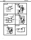
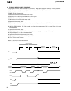
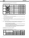
Steps (2) to (12) are illustrated below.
V
PP
V
DD
V
DD
+1
V
DD
V
PP
V
DD
Data input
Data
output
Data input
Write Verify
Additional
data write
Address
increment
X-time repetition
P40-P43
P50-P53
MD0
(P30)
MD1
(P31)
MD2
(P32)
MD3
(P33)
X1