


µ
PD75P308
6
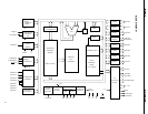
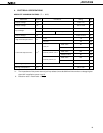
Timer/event counter external event pulse input
Timer/event counter output
Clock output
Fixed frequency output (for buzzer or for trimming
the system clock)
Serial clock input/output
Serial data output
Serial bus input/output
Serial data input
Serial bus input/output
Edge detection vector interrupt input (either rising
or falling edge detection is effective)
Edge detection vector interrupt input (detection
edge can be selected)
Edge detection testable input (rising edge detection)
Testable input/output(parallel falling edge detection)
Testable input/output(parallel falling edge detection)
Segment signal output
Segment signal output
Common signal output
LCD drive power
External dividing resistor disconnect output
Externally expanded driver clock output
Externally expanded driver sync clock output
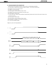
To connect the crystal/ceramic oscillator to the main
system clock generator.
When inputting the external clock, input the external
clock to pin X1, and the reverse phase of the
external clock to pin X2.
To connect the crystal oscillator to the subsystem
clock generator.
When the external clock is used, in XT1 inputs the
external clock. In this case, pin XT2 must be left
open.
Pin XT1 can be used as a 1-bit input (test) pin.
System reset input (low level active)
To select mode when writing/verifying of program
memory (PROM)
Program voltage application when writing and
verifying of program memory (PROM)
Connect to V
DD during the normal operation
Apply +12.5V when writing/verifying EPROM
Positive power supply
GND
—
Input
—
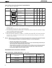
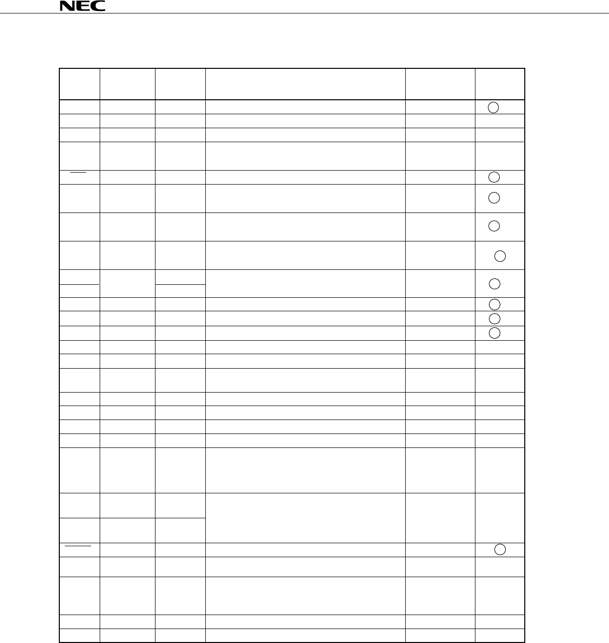
1.2 NON PORT PINS
TI0 Input P13
PTO0 Output P20
PCL Input/Output P22
SCK Input/Output P01
INT0 P10
INT1 P11
INT2 Input P12
KR0-KR3 Input/Output P60-P63
KR4-KR7 Input/Output P70-P73
S0-S23 Output —
S24-S31 Output BP0-7
COM0-
COM3
V
LC0-VLC2 ——
BIAS — —
LCDCL
*2
Input/Output P30
SYNC
*2
Input/Output P31
RESET Input —
MD0-MD3 Input/Output P30-P33
V
DD ——
VSS ——
Input/
Output
Circuit
TYPE
*1
Pin Name
Input/Output Function When Reset
—
Input
Input
Input
—
Input
Input
*3
*3
*3
—
High-impedance
Input
Input
E-B
E-B
BUZ Input/Output P23 Input E-B
F -A
SO/SB0 Input/Output P02 Input
F -B
SI/SB1 Input/Output P03 Input M -C
INT4 Input P00 —
B
Input
B -C
B -C
F -A
F -A
G-A
G-C
G-B
Output —
—
—
E-B
E-B
X1, X2 Input — —
—
—
—
XT1 Input —
XT2 — —
—
E-B
VPP ——
—
—
—
—
—
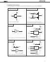
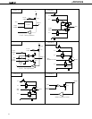
*1: Circles indicate schmitt trigger inputs.
2: These pins are provided for future system expansion. At present, these pins are used only as pins P30 and P31.
3: For these display output, V
LCX indicated below are selected as the input source.
S0 to S31: VLC1, COM0 to COM2: VLC2, COM3: VLC0
However, display output level varies depending on the particular display output and VLCX external circuit.
B
B -C
Also Served
As
★