


Tegra 200 Series Developer Board User Guide
DG-04927-001_v01 Advance Information – Subject to Change 36
NVIDIA CONFIDENTIAL
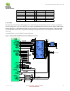
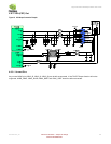
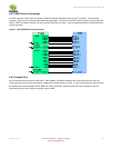
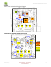
Figure 24. Debug Interface Connection
DBG_RESET_N
VDDIO_SYS
122
11 12
10
2
3
4
5
6
7
8
9
13
14
15
16
17
18
19
20
21
ONKEY_N
10K
10K
100K
Tegra
VDDIO_AUDIO
JTAG_RTCK
VDDIO_SYS
UART
VDDIO_UART
SYSTEM
VDDIO_LCD
AUDIO
LCD
JTAG_TCK
JTAG_TDI
JTAG_TDO
JTAG_TMS
JTAG_TRST_N
UART1_TXD
UART1_RXD
SPI1_SCK
SPI1_CS0_N
SPI1_MOSI
SPI1_MISO
LCD_PWR1
No Stuff
VDDIO_SYS
1.8V
1.8V
1.8V
1.8V
DEBUG
CONNECTOR
DBG_IRQ_N
Unused Pins
If JTAG is not implemented, then JTAG_RTCK and JTAG_TDO can be left unconnected. The JTAG_TDI and JTAG_TMS pins
still need to be pulled up, and JTAG_TRST_N and JTAG_TCK must be pulled down. The rail the JTAG pins reside on
(VDDIO_SYS) must be powered for any mode including Deep Sleep.
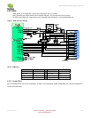
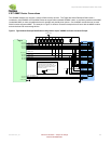
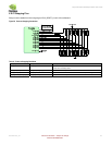
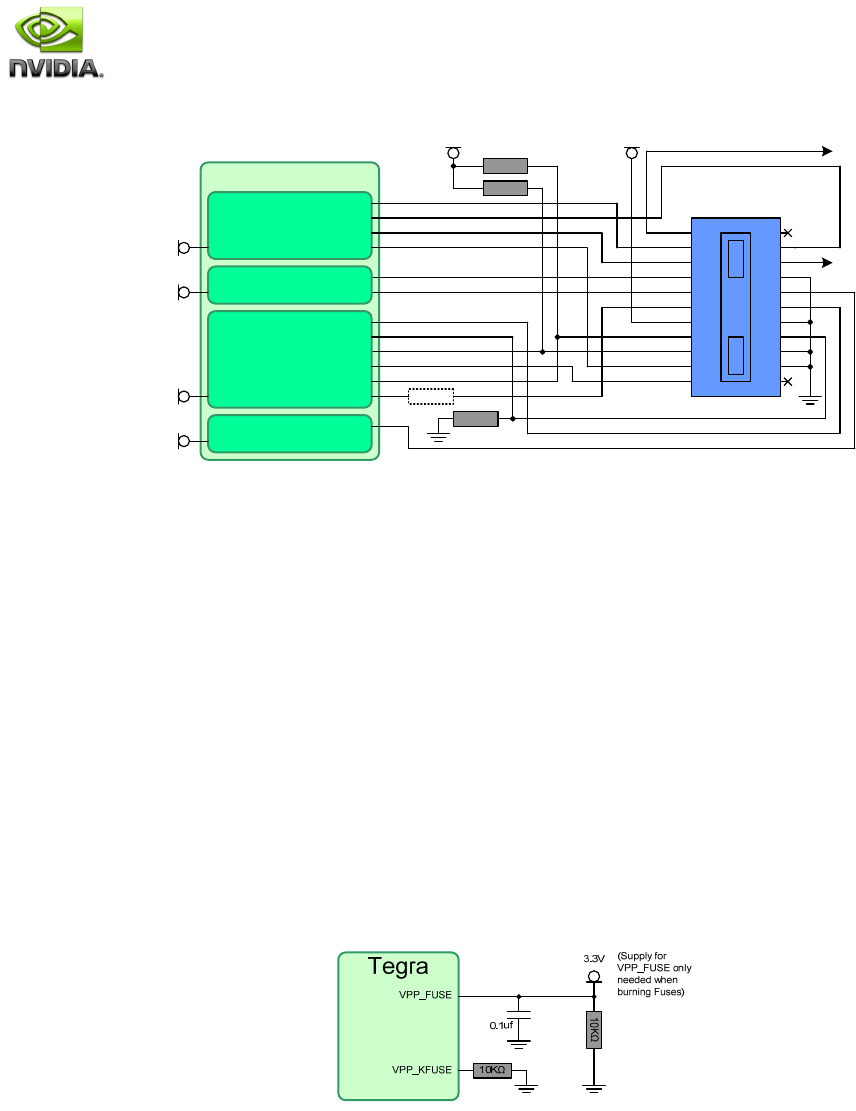
4.9.3 EFUSE
The Tegra 250 design must provide a way to supply a 3.3V power source to the FUSE_SRC pin. This can be accomplished
using one of the following mechanisms:
Test point to connect external 3.3V supply
3.3V Output of on-board LDO controlled by the Tegra 250 GPIO
3.3V Output of PMU, controlled by PWR_I2C from the Tegra 250
Permanently connected to always-on 3.3V supply
The power source must provide a nominal voltage of 3.3V and be able to supply a minimum of 100mA. When not powered, a
10K pull-down resistor each on FUSE_SRC is required. A 0.1uf bypass capacitor is also recommended on FUSE_SRC. The
KFUSE_SRC pin must be pulled down with a 10K resistor only..
Figure 25. EFUSE Connections