


CBT3126_2 © NXP B.V. 2008. All rights reserved.
Product data sheet Rev. 02 — 23 October 2008 3 of 15
NXP Semiconductors
CBT3126
Quad FET bus switch
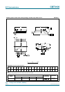
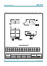
5. Pinning information
5.1 Pinning
5.2 Pin description
6. Functional description
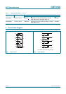
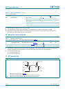
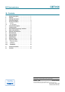
Fig 3. Pin configuration SOT108-1 (SO14), SOT337-4
(SSOP14) and SOT402-1 (TSSOP14)
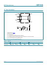
Fig 4. Pin configuration SOT519-1 (SSOP16)
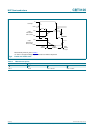
CBT3126
1OE V
CC
1A 4OE
1B 4A
2OE 4B
2A 3OE
2B 3A
GND 3B
001aaj025
1
2
3
4
5
6
7
8
10
9
12
11
14
13
CBT3126
n.c. V
CC
1OE 4OE
1A 4A
1B 4B
2OE 3OE
2A 3A
2B 3B
GND n.c.
001aaj026
1
2
3
4
5
6
7
8
10
9
12
11
14
13
16
15
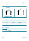
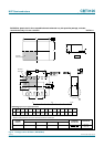
Table 2. Pin description
Symbol Pin SOT108-1 SOT337-4
and SOT402-1
Pin SOT519-1 Description
1OE to 4OE 1, 4, 10, 13 2, 5, 12, 15 output enable input
1A to 4A, 2, 5, 9, 12 3, 6, 11, 14 A input/output
1B to 4B 3, 6, 8, 11 4, 7, 10, 13 B output/input
GND 7 8 ground (0 V)
V
CC
14 16 positive supply voltage
n.c. - 1, 9 not connected
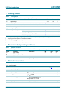
Table 3. Function selection
H = HIGH voltage level; L = LOW voltage level.
Inputs Switch
nOE
L nA to nB disconnected
H nA to nB connected