


CBT3126_2 © NXP B.V. 2008. All rights reserved.
Product data sheet Rev. 02 — 23 October 2008 4 of 15
NXP Semiconductors
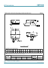
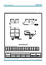
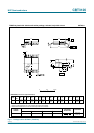
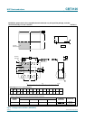
CBT3126
Quad FET bus switch
7. Limiting values
[1] The input and output negative voltage ratings may be exceeded if the input and output clamp current ratings are observed.
[2] The package thermal impedance is calculated from JESD51-7.
[3] For SO14 package; P
tot
derates linearly with 8 mW/K above 70 °C.
[4] For SSOP14, SSOP16 and TSSOP14 packages; P
tot
derates linearly with 5.5 mW/K above 70 °C.
8. Recommended operating conditions
9. Static characteristics
Table 4. Limiting values
In accordance with the Absolute Maximum Rating System (IEC 60134).
Symbol Parameter Conditions Min Max Unit
V
CC
supply voltage −0.5 +7.0 V
V
I
input voltage
[1]
−0.5 +7.0 V
I
CC
supply current continuous current through each V
CC
or GND pin - 128 mA
I
IK
input clamping current V
I
<0V −50 - mA
T
stg
storage temperature −65 +150 °C
P
tot
total power dissipation T
amb
= −40 °C to +125 °C
[2]
SO14 package
[3]
- 500 mW
SSOP14 and SSOP16 package
[4]
- 500 mW
TSSOP14 package
[4]
- 500 mW
Table 5. Operating conditions
All unused control inputs of the device must be held at V
CC
or GND to ensure proper device operation.
Symbol Parameter Conditions Min Max Unit
V
CC
supply voltage 4.5 5.5 V
V
IH
HIGH-level input voltage 2.0 - V
V
IL
LOW-level input voltage - 0.8 V
T
amb
ambient temperature operating in free-air −40 +85 °C
Table 6. Static characteristics
T
amb
=
−
40
°
C to +85
°
C.
Symbol Parameter Conditions Min Typ
[1]
Max Unit
V
IK
input clamping voltage V
CC
= 4.5 V; I
I
= −18 mA - - −1.2 V
V
pass
pass voltage V
I
=V
CC
= 5.0 V; I
O
= −100 µA - 3.8 - V
I
I
input leakage current V
CC
= 5.5 V; V
I
= GND or 5.5 V - - ±1 µA
I
CC
supply current V
CC
= 5.5 V; I
O
= 0 mA;
V
I
=V
CC
or GND
--3µA
∆I
CC
additional supply current control pins; per input;
V
CC
= 5.5 V; one input at 3.4 V,
other inputs at V
CC
or GND
[2]
- - 2.5 mA
C
I
input capacitance control pins; V
I
= 3 V or 0 V - 1.7 - pF
C
io(off)
off-state input/output capacitance V
O
=3V or 0V;OE = V
CC
- 3.4 - pF