


CBT3126_2 © NXP B.V. 2008. All rights reserved.
Product data sheet Rev. 02 — 23 October 2008 7 of 15
NXP Semiconductors
CBT3126
Quad FET bus switch
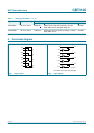
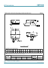
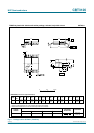
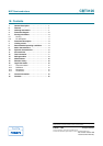
12. Test information
Test data is given in Table 9.
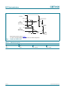
Definitions for test circuit:
R
L
= Load resistance.
C
L
= Load capacitance including jig and probe capacitance.
R
T
= Termination resistance should be equal to the output impedance Z
o
of the pulse generator.
V
EXT
= External voltage for measuring switching times.
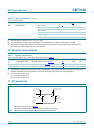
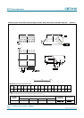
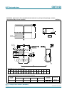
Fig 7. Test circuit for measuring switching times
V
M
V
M
t
W
t
W
10 %
90 %
0 V
V
I
V
I
negative
pulse
positive
pulse
0 V
V
M
V
M
90 %
10 %
t
f
t
r
t
r
t
f
001aae331
V
EXT
V
CC
V
I
V
O
DUT
C
L
R
T
R
L
R
L
G
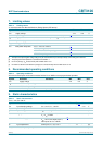
Table 9. Test data
Supply voltage Input Load V
EXT
V
CC
V
I
t
r
, t
f
C
L
R
L
t
PLH
, t
PHL
t
PLZ
, t
PZL
t
PHZ
, t
PZH
4.5 V to 5.5 V GND to 3.0 V ≤ 2.5 ns 50 pF 500 Ω open 7.0 V open