


CBT3126_2 © NXP B.V. 2008. All rights reserved.
Product data sheet Rev. 02 — 23 October 2008 6 of 15
NXP Semiconductors
CBT3126
Quad FET bus switch
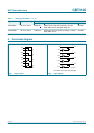
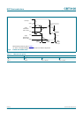
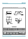
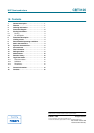
Measurement points are given in Table 8.
V
OL
and V
OH
are typical voltage output levels that occur with the output load.
Fig 6. Enable and disable times
001aaj027
t
PLZ
t
PHZ
switch
disabled
switch
enabled
V
Y
V
X
switch
enabled
output
LOW-to-OFF
OFF-to-LOW
output
HIGH-to-OFF
OFF-to-HIGH
nOE input
V
I
V
OL
V
OH
V
CC
V
M
GND
GND
t
PZL
t
PZH
V
M
V
M
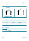
Table 8. Measurement points
Input Output
V
M
V
M
V
X
V
Y
1.5 V 1.5 V V
OL
+ 0.3 V V
OH
− 0.3 V