


CBT3126_2 © NXP B.V. 2008. All rights reserved.
Product data sheet Rev. 02 — 23 October 2008 5 of 15
NXP Semiconductors
CBT3126
Quad FET bus switch
[1] All typical values are measured at V
CC
=5V; T
amb
=25°C.
[2] This is the increase in supply current for each input that is at the specified TTL voltage level rather than V
CC
or GND.
[3] Measured by the voltage drop between the A and the B terminals at the indicated current through the switch. ON resistance is
determined by the lowest voltage of the two (A or B) terminals.
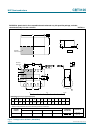
10. Dynamic characteristics
[1] This parameter is warranted but not production tested. The propagation delay is based on the RC time constant of the typical ON
resistance of the switch and a load capacitance, when driven by an ideal voltage source (zero output impedance).
[2] t
PLH
and t
PHL
are the same as t
pd
;
t
PZL
and t
PZH
are the same as t
en
;
t
PLZ
and t
PHZ
are the same as t
dis
.
11. AC waveforms
R
ON
ON resistance V
CC
= 4.0 V
[3]
V
I
= 2.4 V; I
I
= 15 mA - 16 22 Ω
V
CC
= 4.5 V
V
I
=0V; I
I
=64mA - 5 7 Ω
V
I
=0V; I
I
=30mA - 5 7 Ω
V
I
= 2.4 V; I
I
= 15 mA - 10 15 Ω
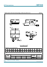
Table 6. Static characteristics
…continued
T
amb
=
−
40
°
C to +85
°
C.
Symbol Parameter Conditions Min Typ
[1]
Max Unit
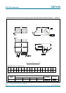
Table 7. Dynamic characteristics
T
amb
=
−
40
°
C to +85
°
C; V
CC
= 4.5 V to 5.5 V; for test circuit see Figure 7.
Symbol Parameter Conditions Min Max Unit
t
pd
propagation delay nA to nB or nB to nA; see Figure 5
[1][2]
- 0.25 ns
t
en
enable time OE to nA or nB; see Figure 6
[2]
1.6 4.5 ns
t
dis
disable time OE to nA or nB; see Figure 6
[2]
1.0 5.4 ns
Measurement points are given in Table 8.
V
OL
and V
OH
are typical voltage output levels that occur with the output load.
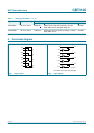
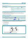
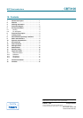
Fig 5. The input (nA, nB) to output (nB, nA) propagation delay times
001aai367
V
M
V
M
V
M
V
M
V
I
input
0 V
V
OH
output
V
OL
t
PHL
t
PLH