


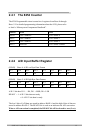
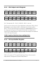
2.4.3 D/A Output Latch Register
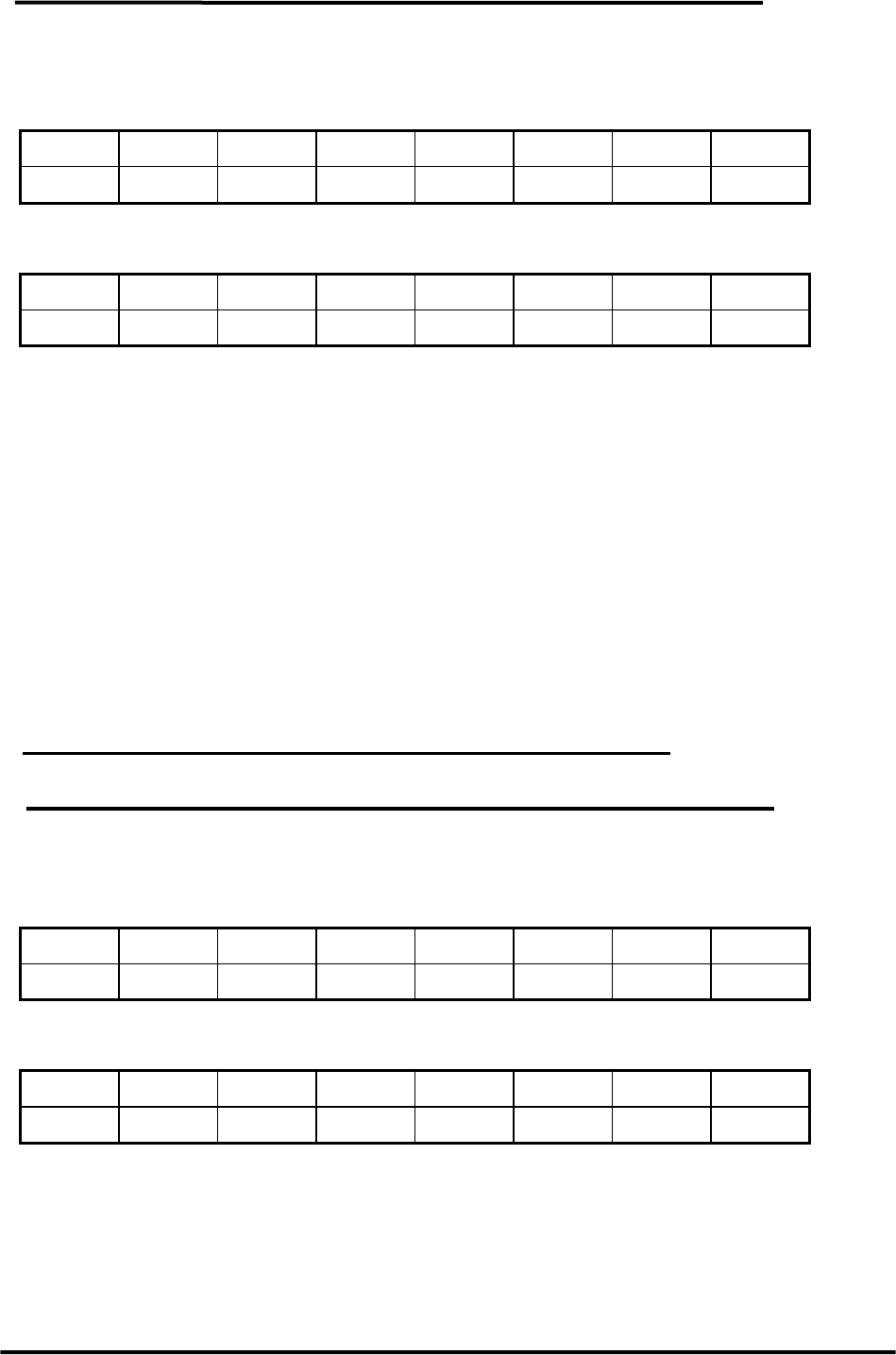
(WRITE) Base+4: Channel 1 D/A Low Byte Data Format
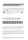
Bit 7 Bit 6 Bit 5 Bit 4 Bit 3 Bit 2 Bit 1 Bit 0
D7 D6 D5 D4 D3 D2 D1 D0
(WRITE) Base+5: Channel 1 D/A High Byte Data Format
Bit 7 Bit 6 Bit 5 Bit 4 Bit 3 Bit 2 Bit 1 Bit 0
X X X X D11 D10 D9 D8
D/A 12 bit output data: D11…D0, D11 = MSB, D0 = LSB, X = don‘t care
The D/A converter will convert the 12 bits of digital data to analog output. The low 8 bits of
D/A channel are stored in address BASE+4 with the high 4 bits are stored in address
BASE+5. The D/A output latch registers are designed as a “double buffered” structure, so
the analog output latch registers will be updated until the high 4 bits of digital data are
written. The users should send the low 8 bits first and then send the high 4 bits to update the
12 bits of AD output latch registers
NOTE: Send low 8 bits first, then send high 4 bits.
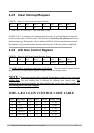
2.4.4 D/I Input Buffer Register
(READ) Base+6: D/I Input Buffer Low Byte Data Format
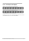
Bit 7 Bit 6 Bit 5 Bit 4 Bit 3 Bit 2 Bit 1 Bit 0
D7 D6 D5 D4 D3 D2 D1 D0
(READ) Base+7: D/I Input Buffer High Byte Data Format
Bit 7 Bit 6 Bit 5 Bit 4 Bit 3 Bit 2 Bit 1 Bit 0
D15 D14 D13 D12 D11 D10 D9 D8
D/I 16 bit input data: D15…D0, D15 = MSB, D0 = LSB
OME-A-8111 provides 16 TTL compatible digital inputs. The low 8 bits are stored in
address BASE+6. The high 8 bits are stored in address BASE+7.
OME-A-8111 Hardware Manual (ver.1.1, Jul/2003) 13