


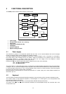
7
1.1 Specifications
•
IN/OUT parameters:
- mV, V, mA, Ω
- Tc type J, K, T, R, S, B, N, C, E, F, U, L, G, D
- Rtd type Pt100, Ni100 and Ni120
•
Reference junction compensation:
- automatic internal with Pt100 sensor from -5°C to +50°C;
- external with manual setting from -50°C to +100°C
•
Rj compensation drift:
± 0.015°C/°C
•
Rj compensation error:
±0.15°C
•
In/Out ranges:
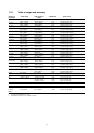
see following tables
•
Resolution:
see following tables
•
Limits of error:
see following tables
•
Common mode rejection:
> 130 dB at 50/60 Hz
•
Normal mode rejection:
> 60 dB at 50/60 Hz
•
Temperature stability:
span ± 0.005% of the reading/°C
zero ± 0.2 µV /°C
•
Output impedance (emf output and Tc):
< 0.5 Ω with maximum current of 0.5 mA
•
Input impedance:
> 10 MΩ (> 1MΩ on 10 V range)
•
Source resistance effect:
1 µV error for 1000 Ω source resistance
•
Rtd and
Ω
ΩΩ
Ω
simulation excitation current:
from 0.2 to 5 mA
•
Rtd and
Ω
ΩΩ
Ω
measurement excitation current:
0.25 mA
•
Rtd cable compensation:
up to 100 Ω (each wire)
•
Shunt resistance (mA ranges):
38 Ω
•
Maximum resistance load:
1000 Ω ( 20mA )
•
Maximum input over voltage dc:
50 V (mV, V, Tc) 5 V (Rtd)
•
Display:
high contrast dot matrix LCD (7x5 dots per character -16 characters)
•
Engineering unit indications:
up to 4 characters shown directly on the display
•
Scale factor:
zero and span programmable within -10000 and +10000
•
Square root:
in combination with scale factor (display limits 0 and +2500)