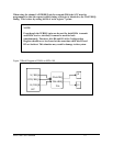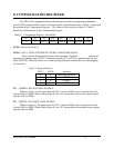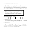
and receive clocks. These clocks can be programmed in WR11 to come from the RTXC pin, the
TRXC pin, the output of the BRG, or the transmit output of the DPLL. Programming of the
clocks should be done before enabling the receiver, transmitter, BRG, or DPLL.
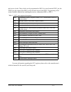
Table 11 SCC write register description.
External/Status interrupt control WR15
Miscellaneous control bits: baud rate generator, DPLL control, auto
echo
WR14
Lower byte of baud rate time constant WR13
Lower byte of baud rate time constant WR12
Clock mode and source controlWR11
Miscellaneous transmitter/receiver control bits, NRZI, NRZ, FM
coding, CRC reset
WR10
Master interrupt control and reset WR9
Transmit bufferWR8
Special HDLC Enhancement Register WR7'
Sync character (2nd byte) or SDLC FlagWR7
Sync character (1st byte) or SDLC address field WR6
Transmitter initialization and control WR5
Transmit/Receive miscellaneous parameters and codes, clock rate,
stop bits, parity
WR4
Receiver initialization and control WR3
Interrupt vectorWR2
Interrupt control, Wait/DMA request controlWR1
Command Register, Register Pointer, CRC initialization, resets for
various modes
WR0
For more information regarding the SCC registers please refer to the manufacturer's
technical manual for the specific part being used.
MPA-100 User's Manual 6-4


