Rev.1.10 Jul 01, 2005 page 10 of 318
REJ09B0124-0110
M16C/6N Group (M16C/6NK, M16C/6NM) 2. Central Processing Unit (CPU)
Under development
This document is under development and its contents are subject to change.
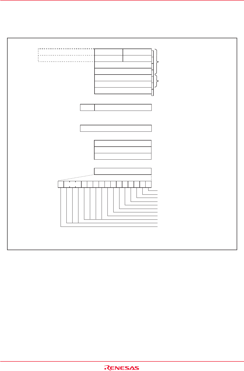
Figure 2.1 CPU Registers
2.1 Data Registers (R0, R1, R2, and R3)
The R0 register consists of 16 bits, and is used mainly for transfers and arithmetic/logic operations. R1 to
R3 are the same as R0.
The R0 register can be separated between high (R0H) and low (R0L) for use as two 8-bit data registers.
R1H and R1L are the same as R0H and R0L. Conversely R2 and R0 can be combined for use as a 32-bit
data register (R2R0). R3R1 is the same as R2R0.
2.2 Address Registers (A0 and A1)
The A0 register consists of 16 bits, and is used for address register indirect addressing and address
register relative addressing. They also are used for transfers and arithmetic/logic operations. A1 is the
same as A0.
In some instructions, A1 and A0 can be combined for use as a 32-bit address register (A1A0).
2. Central Processing Unit (CPU)
Figure 2.1 shows the CPU registers. The CPU has 13 registers. Of these, R0, R1, R2, R3, A0, A1 and FB
comprise a register bank. There are two register banks.
SB
USP
ISP
b15 b0
Static Base Register
User Stack Pointer
Interrupt Stack Pointer
b19 b15
INTBLINTBH
The upper 4 bits of INTB are INTBH and the lower 16 bits of INTB are INTBL.
b0
Interrupt Table Register
b19
PC
b0
Program Counter
R0H (R0's high bits) R0L (R0's low bits)
R1H (R1's high bits) R1L (R1's low bits)
R2
R3
b31 b15 b8 b7 b0
R2
R3
A0
A1
FB
Data Registers
(1)
Address Registers
(1)
Frame Base Registers
(1)
NOTE:
1. These registers comprise a register bank. There are two register banks.
b15 b0
Carry Flag
Debug Flag
Zero Flag
Sign Flag
Register Bank Select Flag
Overflow Flag
Interrupt Enable Flag
Stack Pointer Select Flag
Reserved Area
Processor Interrupt Priority Level
Reserved Area
b15 b0
FLG
Flag Register
IPL U I O B S Z D C
b7b8


