Rev.1.10 Jul 01, 2005 page 279 of 318
REJ09B0124-0110
M16C/6N Group (M16C/6NK, M16C/6NM) 22. Usage Precaution
Under development
This document is under development and its contents are subject to change.
22. Usage Precaution
22.1 SFR
There is the SFR which can not be read (containg bits that will result in unknown data when read).
Please set these registers to their previous values with the instructions other than the read modify write
instructions.
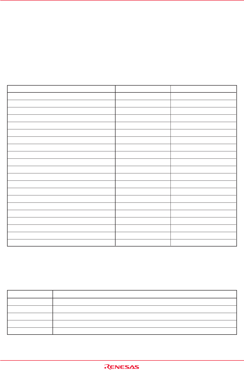
Table 22.1 lists the registers contain bits that will result in unknown data when read and Table 22.2 lists the
instruction table for read modify write.
Table 22.1 Registers Contain Bits that Will Result in Unknown Data When Read
Register Name Symbol Address
Timer A1-1 Register
(1)
TA11 01C3h, 01C2h
Timer A2-1 Register
(1)
TA21 01C5h, 01C4h
Timer A4-1 Register
(1)
TA41 01C7h, 01C6h
Dead Time Timer DTT 01CCh
Timer B2 Interrupt Occurrences Frequency Set Counter
ICTB2 01CDh
SI/O6 Bit Rate Generator
(2)
S6BRG 01D9h
SI/O3 Bit Rate Generator S3BRG 01E3h
SI/O4 Bit Rate Generator S4BRG 01E7h
SI/O5 Bit Rate Generator
(2)
S5BRG 01EBh
UART2 Bit Rate Generator U2BRG 01F9h
UART2 Transmit Buffer Register U2TB 01FBh, 01FAh
Up-Down Flag UDF 0384h
Timer A0 Register
(3)
TA0 0387h, 0386h
Timer A1 Register
(1) (3)
TA1 0389h, 0388h
Timer A2 Register
(1) (3)
TA2 038Bh, 038Ah
Timer A3 Register
(3)
TA3 038Dh, 038Ch
Timer A4 Register
(1) (3)
TA4 038Fh, 038Eh
UART0 Bit Rate Generator U0BRG 03A1h
UART0 Transmit Buffer Register U0TB 03A3h, 03A2h
UART1 Bit Rate Generator U1BRG 03A9h
UART1 Transmit Buffer Register U1TB 03ABh, 03AAh
NOTES:
1. It is affected only in three-phase motor control timer function.
2. These registers are only in the 128-pin version.
3. It is affected only in one-shot timer mode and pulse width modulation mode.
Table 22.2 Instruction Table for Read Modify Write
Function Mnemonic
Bit Manipulation BCLR, BNOT, BSET, BTSTC, BTSTS
Shift RCLC, RORC, ROT, SHA, SHL
Arithmetic ABS, ADC, ADCF, ADD, DEC, EXTS, INC, MUL, MULU, NEG, SBB, SUB
Logical AND, NOT, OR, XOR
Jump ADJNZ, SBJNZ


