


7
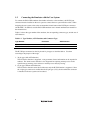
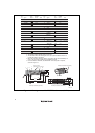
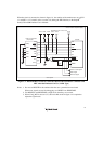
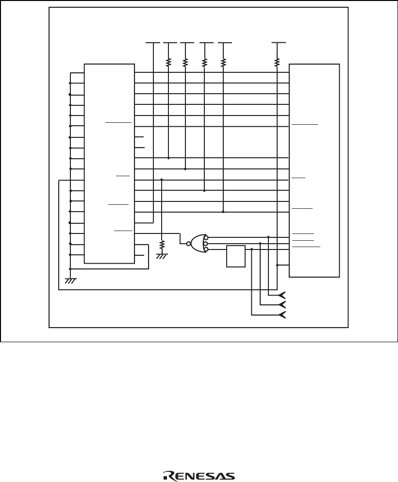
When the circuit is connected as shown in figure 1.3, the switches of the emulator are set as SW2
= 1 and SW3 = 1. For details, refer to section 3.8, Setting the DIP Switches, in the SuperH
TM
Family E10A-USB Emulator User’s Manual.
VccQ
1
AUDATA0
AUDATA2
AUDATA1
AUDATA3
TCK
TMS
AUDSYNC
N.C.
N.C.
RESET
TDI
TDO
TRST
ASEBRK
/ BRKACK
UVCC
GND
GND
GND
GND
(GND)
GND
GND
GND
GND
GND
GND
GND
GND
GND
GND
GND
GND
GND
GND
3
5
7
9
11
13
15
17
19
21
23
25
27
29
31
33
35
2
4
6
8
12
10
14
16
18
20
22
24
26
28
30
32
34
36
AUDATA0
AUDATA2
AUDATA1
AUDATA3
TCK
RESETP
TMS
TDO
TDI
TRST
ASEBRK
/BRKACK
AUDCK
AUDSYNC
AUDCK
N.C.
VccQ
MPMD
VccQ
VccQ
VccQ
VccQ
RESETA
RESETMFI
H-UDI port connector
(36-pin type)
SH7343
Reset signal
Power-on reset signal
MFI reset signal
All pulled-up at 4.7 kΩ or more
1 kΩ
User system
VccQ = 2.85-V I/O power supply
*2
*2
*3
*1
Level-
shift
circuit
Figure 1.3 Recommended Circuit for Connection between the H-UDI Port Connector and
MPU when the Emulator is in Use (36-Pin Type)
Notes: 1. Do not use /RESETP in the emulator after the user system has been activated.
When reset signals are used for debugging, use /RESETA or /RESETMFI.
2. Fix /RESETA and /RESETMFI as high levels when they are not used.
3. When VccQ_MFI is used at 1.8 V, the level-shift circuit in figure 1.3 is required to
adjust the signal levels.