


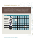

samsung.com/semi/dram
10
1H 2011
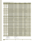
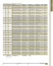
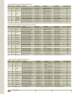
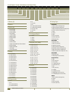
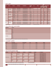
DRAM Ordering Information
1. Memory (K)
2. DRAM: 4
3. DRAM Type
B: DDR3 SDRAM
D: GDDR SDRAM
G: GDDR5 SDRAM
H: DDR SDRAM
J: GDDR3 SDRAM
M: Mobile SDRAM
N: SDDR2 SDRAM
S: SDRAM
T: DDR SDRAM
U: GDDR4 SDRAM
V: Mobile DDR SDRAM Power Efficient Address
W: SDDR3 SDRAM
X: Mobile DDR SDRAM
Y: XDR DRAM
Z: Value Added DRAM
4. Density
10: 1G, 8K/32ms
16: 16M, 4K/64ms
26: 128M, 4K/32ms
28: 128M, 4K/64ms
32: 32M, 2K/32ms
50: 512M, 32K/16ms
51: 512M, 8K/64ms
52: 512M, 8K/32ms
54: 256M, 16K/16ms
55: 256M, 4K/32ms
56: 256M, 8K/64ms
62: 64M, 2K/16ms
64: 64M, 4K/64ms
68: 768M, 8K/64ms
1G: 1G, 8K/64ms
2G: 2G, 8K/64ms
4G: 4G, 8K/64ms
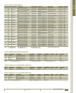
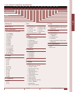
5. Bit Organization
02: x2
04: x4
06: x4 Stack (Flexframe)
07: x8 Stack (Flexframe)
08: x8
15: x16 (2CS)
16: x16
26: x4 Stack (JEDEC Standard)
27: x8 Stack (JEDEC Standard)
30: x32 (2CS, 2CKE)
31: x32 (2CS)
32: x32
6. # of Internal Banks
2: 2 Banks
3: 4 Banks
4: 8 Banks
5: 16 Banks
7. Interface ( VDD, VDDQ)
2: LVTTL, 3.3V, 3.3V
4: LVTTL, 2.5V, 2.5V
5: SSTL-2 1.8V, 1.8V
6: SSTL-15 1.5V, 1.5V
8: SSTL-2, 2.5V, 2.5V
A: SSTL, 2.5V, 1.8V
F: POD-15 (1.5V,1.5V)
H: SSTL_2 DLL, 3.3V, 2.5V
M: LVTTL, 1.8V, 1.5V
N: LVTTL, 1.5V, 1.5V
P: LVTTL, 1.8V, 1.8V
Q: SSTL-2 1.8V, 1.8V
R: SSTL-2, 2.8V, 2.8V
U: DRSL, 1.8V, 1.2V
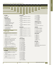
8. Revision
A: 2nd Generation
B: 3rd Generation
C: 4th Generation
D: 5th Generation
E: 6th Generation
F: 7th Generation
G: 8th Generation
H: 9th Generation
I: 10th Generation
J: 11th Generation
K: 12th Generation
M: 1st Generation
N: 14th Generation
Q: 17th Generation
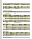
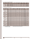
9. Package Type
DDR SDRAM
L: TSOP II (Lead-free & Halogen-free)
H: FBGA (Lead-free & Halogen-free)
F: FBGA for 64Mb DDR (Lead-free & Halogen-free)
6: sTSOP II (Lead-free & Halogen-free)
T: TSOP II
N: sTSOP II
G: FBGA
U: TSOP II (Lead-free)
V: sTSOP II (Lead-free)
Z: FBGA (Lead-free)
DDR2 SDRAM
Z: FBGA (Lead-free)
J: FBGA DDP (Lead-free)
Q: FBGA QDP (Lead-free)
H: FBGA (Lead-free & Halogen-free)
M: FBGA DDP (Lead-free & Halogen-free)
E: FBGA QDP (Lead-free & Halogen-free)
T: FBGA DSP (Lead-free & Halogen-free, Thin)
DDR3 SDRAM
Z: FBGA (Lead-free)
H: FBGA (Halogen-free & Lead-free)
Graphics Memory
Q: TQFP
U: TQFP (Lead Free)
G: 84/144 FBGA
V: 144 FBGA (Lead Free)
Z: 84 FBGA(Lead Free)
T: TSOP
L: TSOP (Lead Free)
A: 136 FBGA
B: 136 FBGA(Lead Free)
H: FBGA(Hologen Free & Lead Free)
E: 100 FBGA(Hologen Free & Lead Free)
SDRAM
L TSOP II (Lead-free & Halogen-free)
N: STSOP II
T: TSOP II
U: TSOP II (Lead-free)
V: sTSOP II (Lead-free)
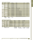
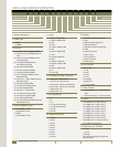
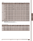
COMPONENT DRAM ORDERING INFORMATION
1 2 3 4 5 6 7 8 9 10 11
K 4 T XX XX X X X X X XX
SAMSUNG Memory
DRAM
DRAM Type
Density
Bit Organization
Speed
Temp & Power
Package Type
Revision
Interface (VDD, VDDQ)
Number of Internal Banks