


samsung.com/semi/dram
12
1H 2011
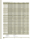
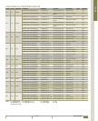
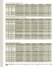
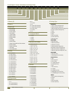
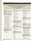
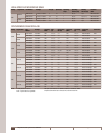
DRAM Ordering Information
1. Memory Module: M
2. DIMM Type
3: DIMM
4: SODIMM
3. Data bits
12: x72 184pin Low Profile Registered DIMM
63: x63 PC100 / PC133 SODIMM with SPD for
144pin
64: x64 PC100 / PC133 SODIMM with SPD for
144pin (Intel/JEDEC)
66: x64 Unbuffered DIMM with SPD for
144pin/168pin (Intel/JEDEC)
68: x64 184pin Unbuffered DIMM
70: x64 200pin Unbuffered SODIMM
71: x64 204pin Unbuffered SODIMM
74: x72 /ECC Unbuffered DIMM with SPD for
168pin (Intel/JEDEC)
77: x72 /ECC PLL + Register DIMM with SPD for
168pin (Intel PC100)
78: x64 240pin Unbuffered DIMM
81: x72 184pin ECC unbuffered DIMM
83: x72 184pin Registered DIMM
90: x72 /ECC PLL + Register DIMM
91: x72 240pin ECC unbuffered DIMM
92: x72 240pin VLP Registered DIMM
93: x72 240pin Registered DIMM
95: x72 240pin Fully Buffered DIMM with SPD for
168pin (JEDEC PC133)
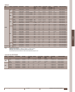
4. DRAM Component Type
B: DDR3 SDRAM (1.5V VDD)
L: DDR SDRAM (2.5V VDD)
S: SDRAM
T: DDR2 SDRAM (1.8V VDD)
5. Depth
09: 8M (for 128Mb/512Mb)
17: 16M (for 128Mb/512Mb)
16: 16M
28: 128M
29: 128M (for 128Mb/512Mb)
32: 32M
33: 32M (for 128Mb/512Mb)
51: 512M
52: 512M (for 512Mb/2Gb)
56: 256M
57: 256M (for 512Mb/2Gb)
59: 256M (for 128Mb/512Mb)
64: 64M
65: 64M (for 128Mb/512Mb)
1G: 1G
1K: 1G (for 2Gb)
6. # of Banks in Comp. & Interface
1: 4K/64mxRef., 4Banks & SSTL-2
2 : 8K/ 64ms Ref., 4Banks & SSTL-2
2: 4K/ 64ms Ref., 4Banks & LVTTL (SDR Only)
5: 8K/ 64ms Ref., 4Banks & LVTTL (SDR Only)
5: 4Banks & SSTL-1.8V
6: 8Banks & SSTL-1.8V
7. Bit Organization
0: x 4
3: x 8
4: x16
6: x 4 Stack (JEDEC Standard)
7: x 8 Stack (JEDEC Standard)
8: x 4 Stack
9: x 8 Stack
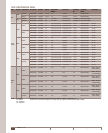
8. Component Revision
A: 2nd Gen.
B: 3rd Gen.
C: 4th Gen.
D: 5th Gen.
E: 6th Gen.
F: 7th Gen.
G: 8th Gen.
M: 1st Gen.
Q: 17th Gen.
9. Package
E: FBGA QDP (Lead-free & Halogen-free)
G: FBGA
H: FBGA (Lead-free & Halogen-free)
J: FBGA DDP (Lead-free)
M: FBGA DDP (Lead-free & Halogen-free)
N: sTSOP
Q: FBGA QDP (Lead-free)
T: TSOP II (400mil)
U: TSOP II (Lead-Free)
V: sTSOP II (Lead-Free)
Z: FBGA(Lead-free)
10. PCB Revision
0: Mother PCB
1: 1st Rev
2: 2nd Rev.
3: 3rd Rev.
4: 4th Rev.
A: Parity DIMM
S: Reduced PCB
U: Low Profile DIMM
11. Temp & Power
C: Commercial Temp. (0°C ~ 95°C) & Normal
Power
L: Commercial Temp. (0°C ~ 95°C) & Low Power
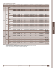
12. Speed
CC: (200MHz @ CL=3, tRCD=3, tRP=3)
D5: (266MHz @ CL=4, tRCD=4, tRP=4)
E6: (333MHz @ CL=5, tRCD=5, tRP=5)
F7: (400MHz @ CL=6, tRCD=6, tRP=6)
E7: (400MHz @ CL=5, tRCD=5, tRP=5)
F8: (533MHz @ CL=7, tRCD=7, tRP=7)
G8: (533MHz @ CL=8, tRCD=8, tRP=8)
H9: (667MHz @ CL=9, tRCD=9, tRP=9)
K0: (800MHz @ CL=10, tRCD=10, tRP=10)
7A: (133MHz CL=3/PC100 CL2)
13. AMB Vendor for FBDIMM
0, 5: Intel
1, 6, 8: IDT
9: Montage
Note: All of Lead-free or Halogen-free product are in
compliance with RoHS
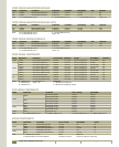
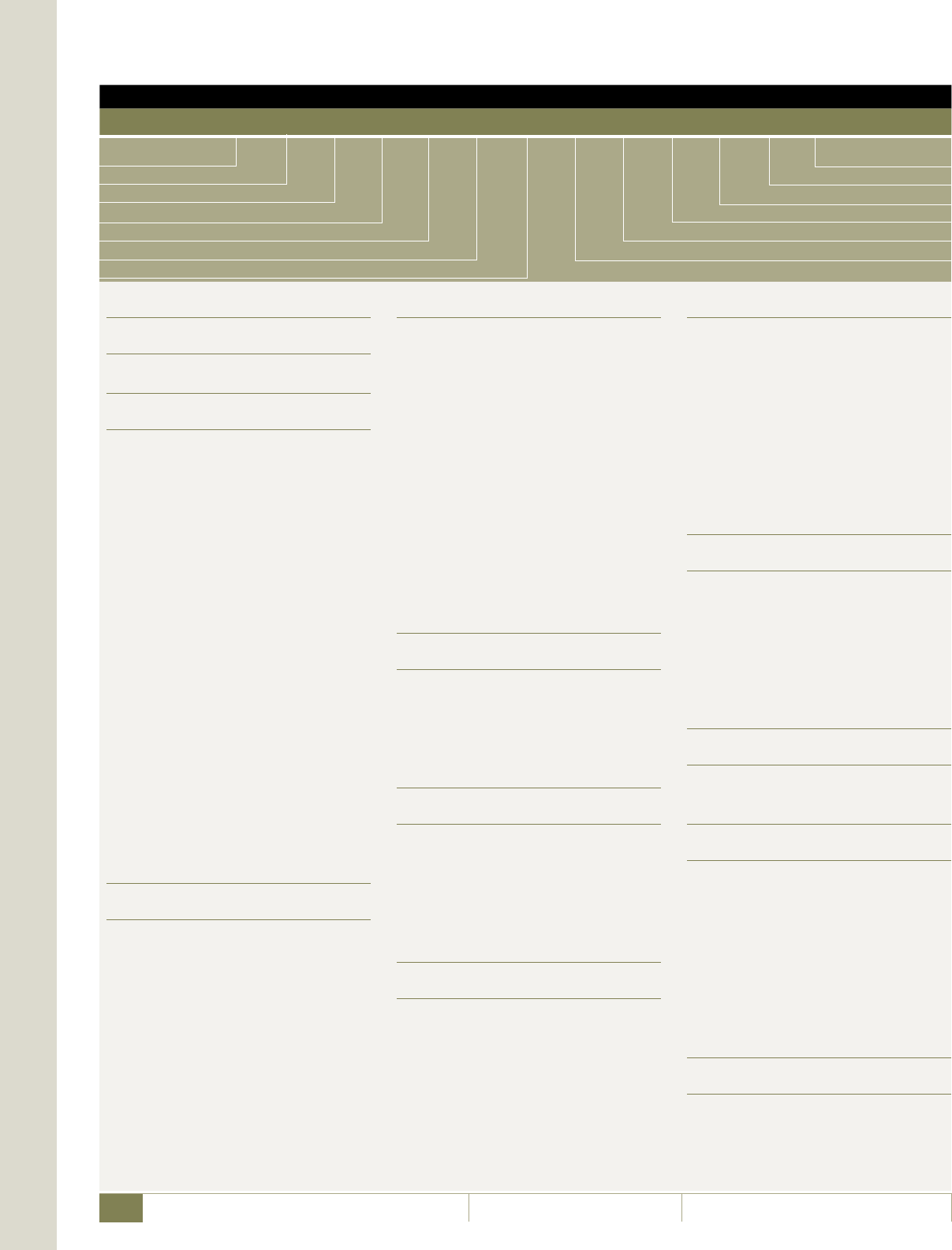
MODULE DRAM ORDERING INFORMATION
1 2 3 4 5 6 7 8 9 10 11 12 13
M X XX T XX X X X X X X XX X
SAMSUNG Memory
DIMM
Data bits
DRAM Component Type
Depth
Number of Banks
Bit Organization
AMB Vendor
Speed
Temp & Power
PCB Revision
Package
Component Revision