


SanDisk CompactFlash Card OEM Product Manual Interface Description
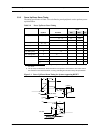
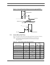
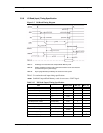
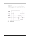
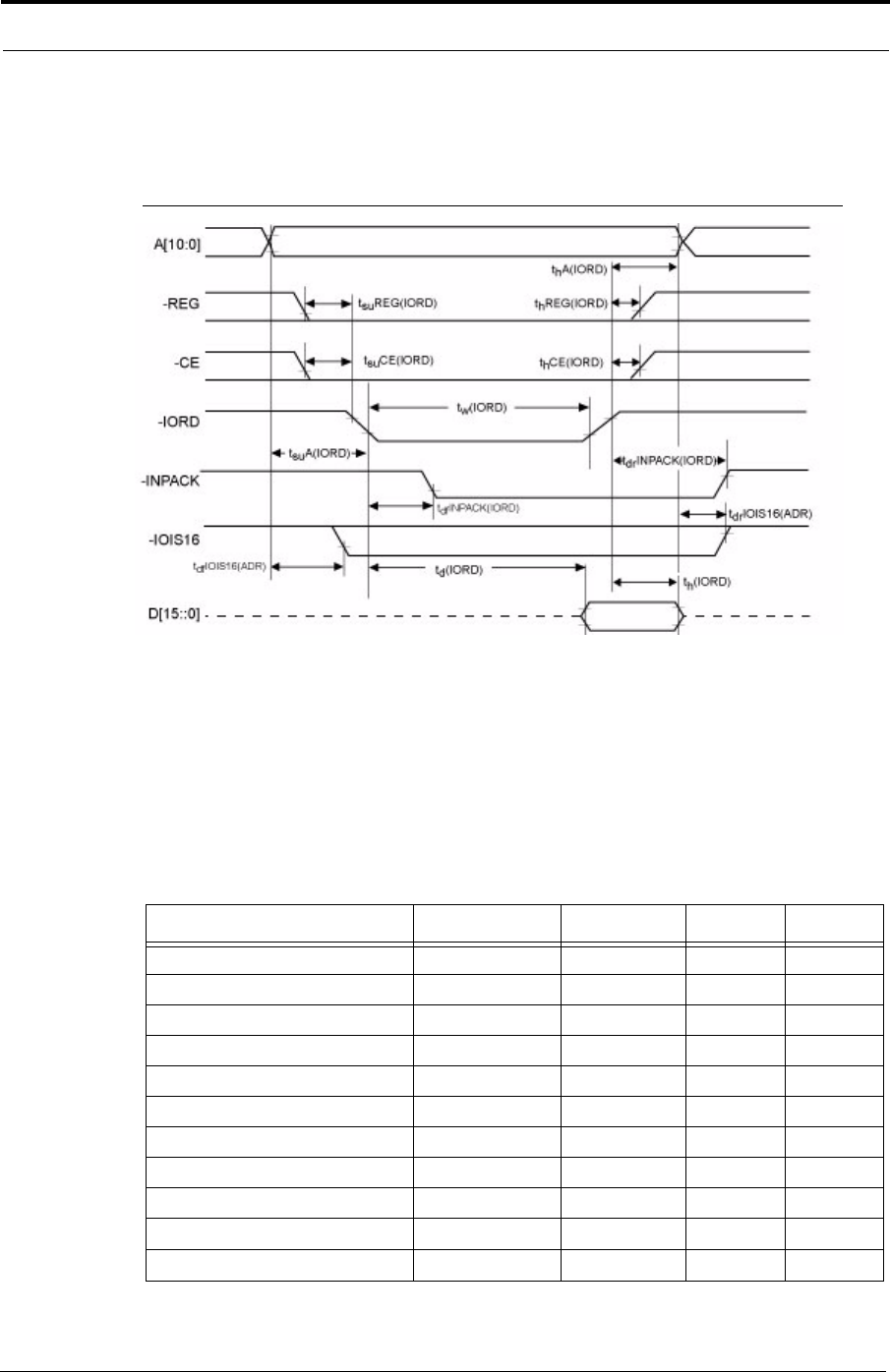
3.3.8 I/O Read (Input) Timing Specification
Figure 3-5 I/O Read Timing Diagram
NOTE 1: All timings are measured at the CompactFlash Memory Card.
NOTE 2: Skews and delays from the host system driver/receiver to the card must be
accounted for by the system design.
NOTE 3: D[15::0] signifies data provided by the card to the host system.
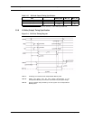
Table 3-13 contains the read input timing specifications.
NOTE: SanDisk CompactFlash Memory cards do ont assert a -WAIT signal.
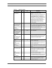
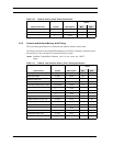
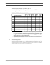
Table 3-13 I/O Read (Input) Timing Specification
Item
Symbol
IEEE Symbol Min. (ns) Max. (ns)
Data Delay after -IORD t
d
(IORD) tl
GLQV
--- 100
Data Hold following -IORD t
h
(IORD) tl
GHQX
0 ---
-IORD Width Time t
w
(IORD) tl
GLIGH
165 ---
Address Setup before -IORD t
su
A(IORD) t
AVIGL
70 ---
Address Hold following -IORD t
h
A(IORD) tl
GHAX
20 ---
-CE Setup before -IORD t
su
CE(IORD) t
ELIGL
5 ---
-CE Hold following -IORD t
h
CE(IORD) tl
GHEH
20 ---
-REG Setup before -IORD t
su
REG(IORD) t
RGLIGL
5 ---
-REG Hold following -IORD t
h
REG(IORD) tl
GHRGH
0 ---
-INPACK Delay falling from -IORD t
df
INPACK(IORD) tl
GLIAL
0
45
a
-INPACK Delay rising from -IORD t
dr
INPACK(IORD) tl
GHIAH
---
45
a
© 2007 SanDisk Corporation 3-15 Rev. 12.0, 02/07