


SanDisk CompactFlash Card OEM Product Manual ATA Register Set and Protocol
Card (Drive) Address Register (con’t)
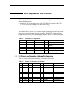
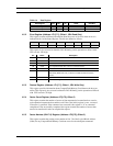
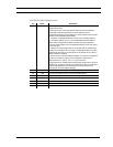
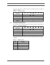
Bit Name Description
D7 X This bit is unknown.
Implementation Note:
Conflicts may occur on the host data bus when this bit is provided by a
Floppy Disk Controller operating at the same addresses as the
CompactFlash Memory Card. Following are some possible solutions to this
problem for the PCMCIA implementation:
1. Locate the CompactFlash Memory Card at a non-conflicting address,
i.e., Secondary address (377) or in an independently decoded Address
Space when a Floppy Disk Controller is located at primary addresses.
2. Do not install a Floppy and a CompactFlash Memory Card in the system
at the same time
3. Implement a socket adapter that can be programmed to (conditionally)
tri-state D7 of I/0 address 3F7/377 when a CompactFlash Memory Card is
installed and conversely to tri-state D6-D0 of I/O address 3F7/377 when a
floppy controller is installed
4. Do not use the card's Drive Address Register. This may be accomplished
by either a) If possible, program the host adapter to enable only I/O
addresses 1F0-1F7, 3F6 (or 170-177, 176) to the card or
b) if provided use an additional primary/secondary configuration in the card
that does not respond to accesses to I/O locations 3F7 and 377. With either
of these implementations, the host software must not attempt to use
information in the Drive Address Register.
D6 -WTG This bit is 0 when a write operation is in progress, otherwise, it is 1.
D5 -HS3 This bit is the negation of bit 3 in the Drive/Head Register.
D4 -HS2 This bit is the negation of bit 2 in the Drive/Head Register.
D3 -HS1 This bit is the negation of bit 1 in the Drive/Head Register.
D2 -HS0 This bit is the negation of bit 0 in the Drive/Head Register.
D1 -nDS1 This bit is 0 when drive 1 is active and selected.
D0 -nDS0 This bit is 0 when the drive 0 is active and selected.
© 2007 SanDisk Corporation 4-9 Rev. 12.0, 02/07