


ATA Register Set and Protocol SanDisk CompactFlash Card OEM Product Manual
a. Register 0 is accessed with -CE1 low and -CE2 low (and A0 = Do not care) as a word register on the
combined Odd Data Bus and Even Data Bus (D15-D0). This register may also be accessed by a pair
of byte accesses to the offset 0 with -CE1 low and -CE2 high. Note that the address space of this
word register overlaps the address space of the Error and Feature byte-wide registers that lie at off-
set 1. When accessed twice as byte register with CE1 low, the first byte to be accessed is the even
byte of the word and the second byte accessed is the odd byte of the equivalent word access.
b. A byte access to register 0 with CE1 high and CE2 low accesses the error (read) or feature (write)
register.
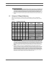
4.2 Contiguous I/O Mapped Addressing
When the system decodes a contiguous block of I/O registers to select a CompactFlash
Memory Card, the registers are accessed in the block of I/O space decoded by the system as
follows:
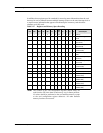
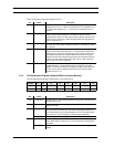
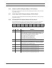
Table 4-3 Contiguous I/O Decoding
-REG A3 A2 A1 A0 Offset -IORD=0 -IOWR=0
0 0 0 0 0 0
Even RD Data
a
Even WR Data
a
0 0 0 0 1 1
Error Register
b
Features
b
0 0 0 1 0 2 Sector Count Sector Count
0 0 0 1 1 3 Sector No. Sector No.
0 0 1 0 0 4 Cylinder Low Cylinder Low
0 0 1 0 1 5 Cylinder High Cylinder High
0 0 1 1 0 6 Select Card/Head Select Card/Head
0 0 1 1 1 7 Status Command
0 1 0 0 0 8
Dup Even RD Data
b
Dup Even WR Data
b
0 1 0 0 1 9
Dup Odd RD Data
b
Dup Odd WR Data
b
0 1 1 0 1 D
Dup Error
b
Dup Features
b
0 1 1 1 0 E Alt Status Device Ctl
0 1 1 1 1 F Drive Address Reserved
a. Register 0 is accessed with -CE1 low and -CE2 low (and A0 = Do not care) as a word register on the
combined Odd Data Bus and Even Data Bus (D15-D0). This register may also be accessed by a pair
of byte accesses to the offset 0 with -CE1 low and -CE2 high. Note that the address space of this
word register overlaps the address space of the Error and Feature byte-wide registers that lie at off-
set 1. When accessed twice as byte register with CE1 low, the first byte to be accessed is the even
byte of the word and the second byte accessed is the odd byte of the equivalent word access. A
byte access to register 0 with CE1 high and CE2 low accesses the error (read) or feature (write)
register.
b. Registers at offset 8, 9 and D are non-overlapping duplicates of the registers at offset 0 and 1.
Register 8 is equivalent to register 0, while register 9 accesses the odd byte. Therefore, if the regis-
ters are byte accessed in the order 9 then 8 the data will be transferred odd byte then even byte.
Repeated byte accesses to register 8 or 0 will access consecutive (even than odd) bytes from the
data buffer. Repeated word accesses to register 8, 9 or 0 will access consecutive words from the
data buffer. Repeated byte accesses to register 9 are not supported. However, repeated alternating
byte accesses to registers 8 then 9 will access consecutive (even then odd) bytes from the data
buffer. Byte accesses to register 9 access only the odd byte of the data.
02/07, Rev. 12.0 4-2 © 2007 SanDisk Corporation