


Interface Description SanDisk CompactFlash Card OEM Product Manual
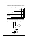
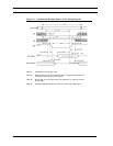
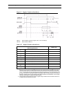
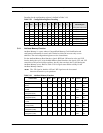
Figure 3-7 Register Transfer to/from Device
NOTE 1: Device address consists of signals -CS0, -CS1 and -DA(2:0).
NOTE 2: Data consists of DD(7:0).
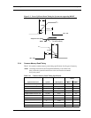
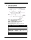
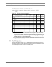
Table 3-15 Register Transfer to/from Device
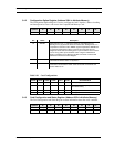
PIO Timing Parameters
Mode 4 (ns)
t
0
a
Cycle time (min.) 120
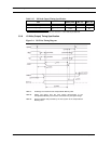
t
1
Address valid to IORD-/IOWR- setup (min.) 25
t
2
a
IORD-/IOWR- pulse width 8-bit (min.) 70
t
2i
a
IORD-/IOWR- recovery time (min.) 25
t
3
IOWR- data setup (min.) 20
t
4
IOWR- data hold (min.) 10
t
5
IORD- data setup (min.) 20
t
6
IORD- data hold (min.) 5
t
6z
b
IORD- data tri-state (max.) 30
t
9
IORD-/IOWR- to address valid hold (min.) 10
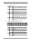
a. t
0
is the minimum total cycle time, t
2
is the minimum command active time, and t
2i
is the minimum
command recovery time or command inactive time. The actual cycle time equals the sum of the
actual command active time and the actual command inactive time. The three timing requirements
of t
0
, t
2
, and t
2i
shall be met. The minimum total cycle time requirements are greater than the sum of
t
2
and t
2i
. This means a host implementation may lengthen either or both t
2
or t
2i
to ensure that t
0
is
equal to or greater than the value reported in the devices IDENTIFY DEVICE data. A device imple-
mentation shall support any legal host implementation.
b. This parameter specifies the time from the negation edge of /IORD to the time that the data bus is
no longer driven by the device (tri-state).
02/07, Rev. 12.0 3-18 © 2007 SanDisk Corporation