AN.No.G1216B1N000-3D0E
- 15 -
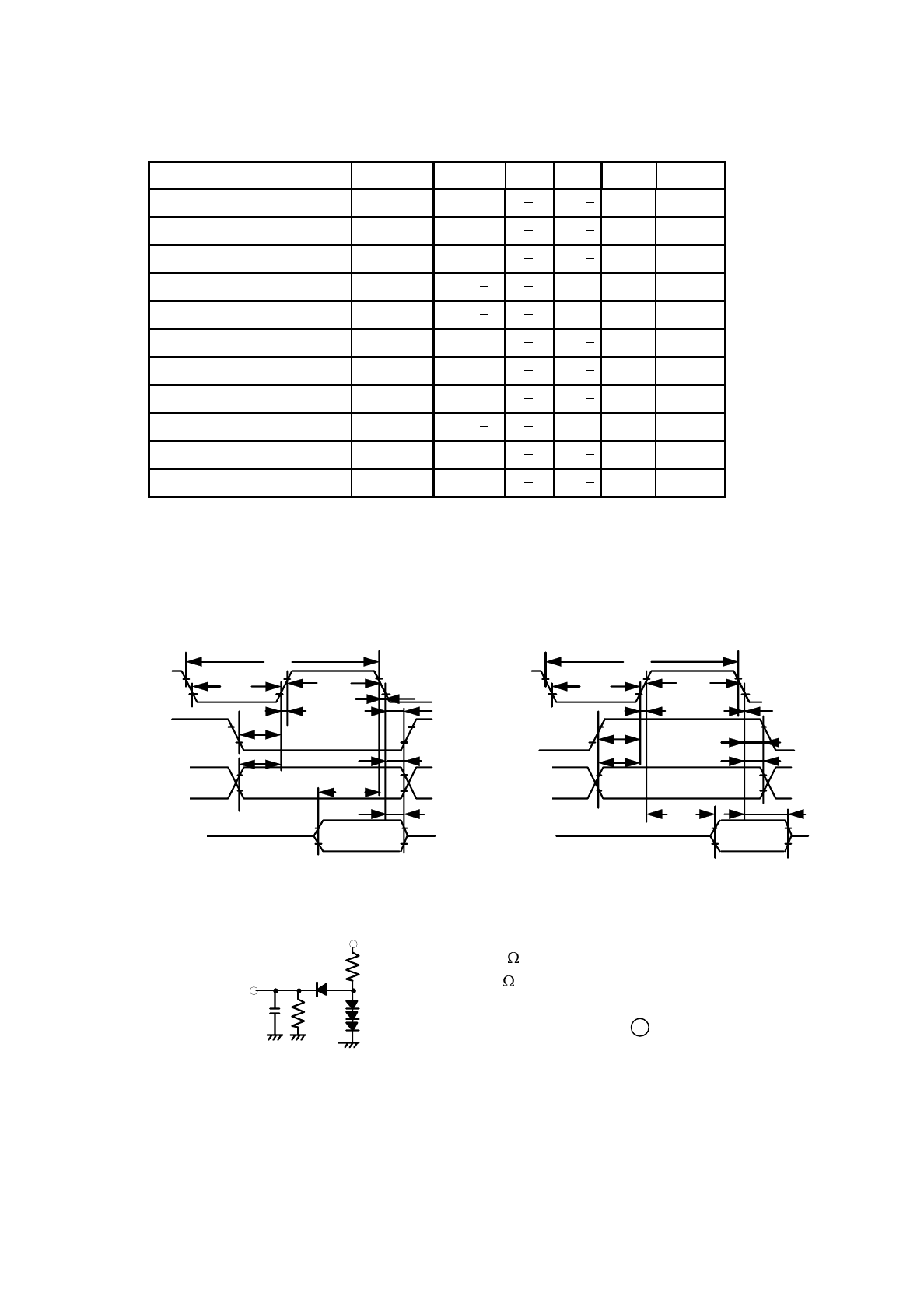
3.2 Timing Characteristics
t
f
t
CYC
t
CYC
R / W
2.4V
0.4V
t
DDR
t
DHR
t
AH
t
AH
2.0V
0.8V
t
AS
t
AS
2.0V
0.8V
t
DHW
t
DSW
t
AS
t
AS
2.0V
0.8V
t
AH
t
AH
t
r
2.0V
0.8V
P
WEL
2.0V
0.8V
P
WEH
D
1
Test point
C R
R
L
D
2
D
3
D
4
25
25
320
1000
450
450
140
10
200
10
20
t
CYC
P
WEH
P
WEL
t
r
t
f
t
AS
t
AH
t
DSW
t
DDR
t
DHW
t
DHR
ns
ns
ns
ns
ns
ns
ns
ns
ns
ns
ns
1, 2
1, 2
1, 2
1, 2
1, 2
1, 2
1, 2
1
2, 3
1
2
E cycle time
E pulse width (H)
E pulse width (L)
E rise time
E fall time
Address setup time
Address hold time
Data setup time
Data delay time
Data hold time during write
Data hold time during read
NoteunitMax.Typ.Min.SymbolItem
Note 1: When the MPU writes:
Note 3: Load circuits (DB
0
to DB
7
)
E
t
f
t
r
P
WEL
2.0V
0.8V
P
WEH
Note 2: When the MPU reads:
DB
0
to DB
7
R
L
= 2.4 k
R=11 k
C = 130 pF (including jig capacity)
Diodes D1 to D4 are 1S2074 H .
E
DB
0
to DB
7
R / W
CS1, CS2
D/I
CS1, CS2
D/I
2.0V
0.8V


