SILICONSYSTEMS PROPRIETARY
This document and the information contained within it is confidential and proprietary to SiliconSystems, Inc.
All unauthorized use and/or reproduction is prohibited.
PAGE 8JUNE 17, 2008 DOCUMENT: 3650H-02DSR
SSD-HXXX(I)-3650 DATA SHEET ELECTRICAL SPECIFICATION
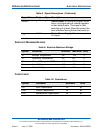
ABSOLUTE MAXIMUM RATINGS
CAPACITANCE
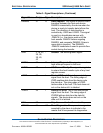
-RESET 1 I Device Reset. An active low signal. When
active, this signal sets all internal registers
to their default state. This signal is held
asserted until at least 25μs after power has
been stabilized during the device power-on.
V
CC
41, 42 - Device Power Supply. The device power
5V signal.
Table 8: Signal Descriptions (Continued)
Signal Name Pin(s) Type Description
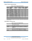
Table 9: Absolute Maximum Ratings
Symbol Parameter Minimum Maximum Units
Ts Storage Temperature -55 125 °C
T
A
Operating Temperature -40 85 °C
V
CC
V
CC
with Respect to GND -0.3 6.7 V
Vin Input Voltage -0.5 6.0 V
Vout Output Voltage -0.3 5.8 V
Table 10: Capacitance
Symbol Parameter Maximum Units
Cin Input Capacitance 35 pF
Cout Output Capacitance 35 pF
CI/O Bidirectional Capacitance 35 pF


