


Si53xx-RM
102 Rev. 0.5
7.13. I
2
C Serial Microprocessor Interface
When configured in I
2
C control mode (CMODE = L), the control interface to the device is a 2-wire bus for
bidirectional communication. The bus consists of a bidirectional serial data line (SDA) and a serial clock input
(SCL). Both lines must be connected to the positive supply via an external pull-up. In addition, an output interrupt
(INT) is provided with selectable active polarity (determined by INT_POL bit). Fast mode operation is supported for
transfer rates up to 400 kbps as specified in the I
2
C-Bus Specification standard. To provide bus address flexibility,
three pins (A[2:0]) are available to customize the LSBs of the device address. The complete bus address for the
device is as follows:
1 1 0 1 A[2] A[1] A[0] R/W.
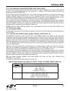
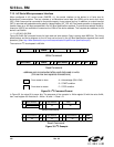
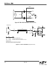
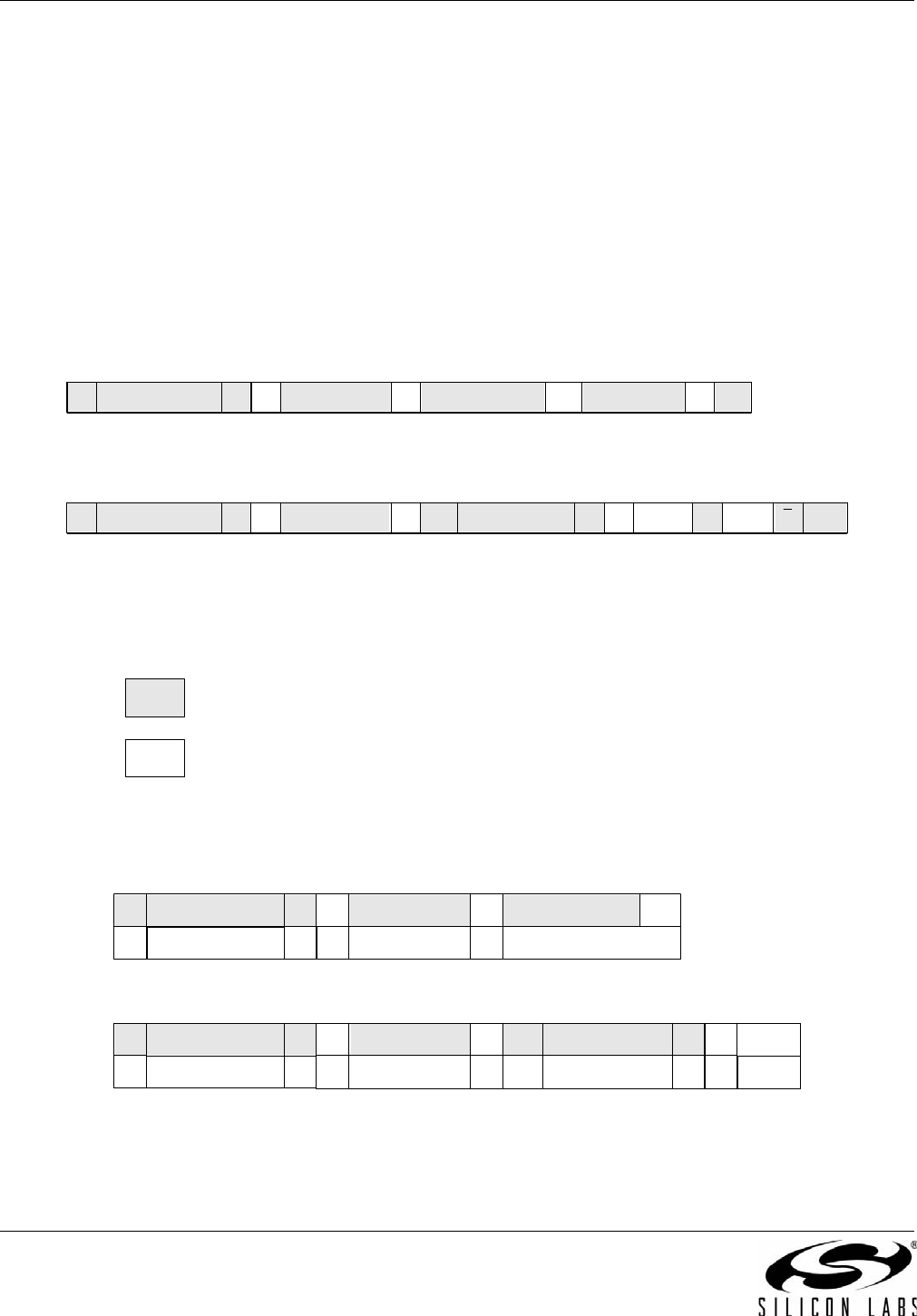
Figure 34 shows the command format for both read and write access. Data is always sent MSB first. The timing
specifications and timing diagram for the I
2
C bus can be found in the I
2
C-Bus Specification standard (fast mode
operation) (See: http://www.standardics.nxp.com/literature/books/i2c/pdf/i2c.bus.specification.pdf).
The maximum I
2
C clock speed is 400 kHz.
Figure 34. I
2
C Command Format
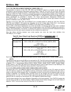
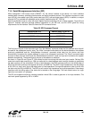
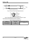
In Figure 35, the value 68 is seven bits. The sequence of the example is: Write register 00 with the value 0xAA;
then, read register 00. Note that 0 = Write = W, and 1 = Read = R.
Figure 35. I
2
C Example
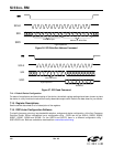
AData AData PA1Slave AddressSA
Byte
Address
A0Slave AddressS AData AData P1Slave AddressSA
Byte
Address
A0Slave AddressS
From master to slave
From slave to master
A – Acknowledge (SDA LOW)
S
– START condition
P
– STOP condition
Write Command
Read Command
–address auto incremented after each data read or write
(this can be two separate transactions)
PADataADataA
Byte
Address
A0Slave AddressS PADataADataA
Byte
Address
A0Slave AddressS
AData1Slave AddressSA
Byte Address
A0Slave AddressS Data0
Write Command
Read Command
ADataAByte AddressA0Slave AddressS
68
W
00
68
R
AA
68
W
00
AA