


Si53xx-RM
50 Rev. 0.5
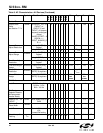
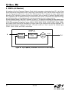
6. Pin Control Parts (Si5316, Si5322, Si5323, Si5365, Si5366)
These parts provide high-performance clock multiplication with simple pin control. Many of the control inputs are
three levels: High, Low, and Medium. High and Low are standard voltage levels determined by the supply voltage:
V
DD
and Ground. If the input pin is left floating, it is driven to nominally half of V
DD
. Effectively, this creates three
logic levels for these controls.
These parts span a range of applications and I/O capacity as shown in Table 12.
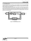
6.1. Clock Multiplication (Si5316, Si5322, Si5323, Si5365, Si5366)
By setting the tri-level FRQSEL[3:0] pins these devices provide a wide range of standard SONET and data
communications frequency scaling, including simple integer frequency multiplication to fractional settings required
for coding and decoding.
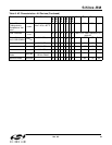
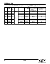
6.1.1. Clock Multiplication (Si5316)
The device accepts dual input clocks in the 19, 39, 78, 155, 311, or 622 MHz frequency range and generates a de-
jittered output clock at the same frequency. The frequency range is set by the FRQSEL [1:0] pins, as shown in
Table 13.
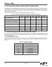
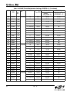
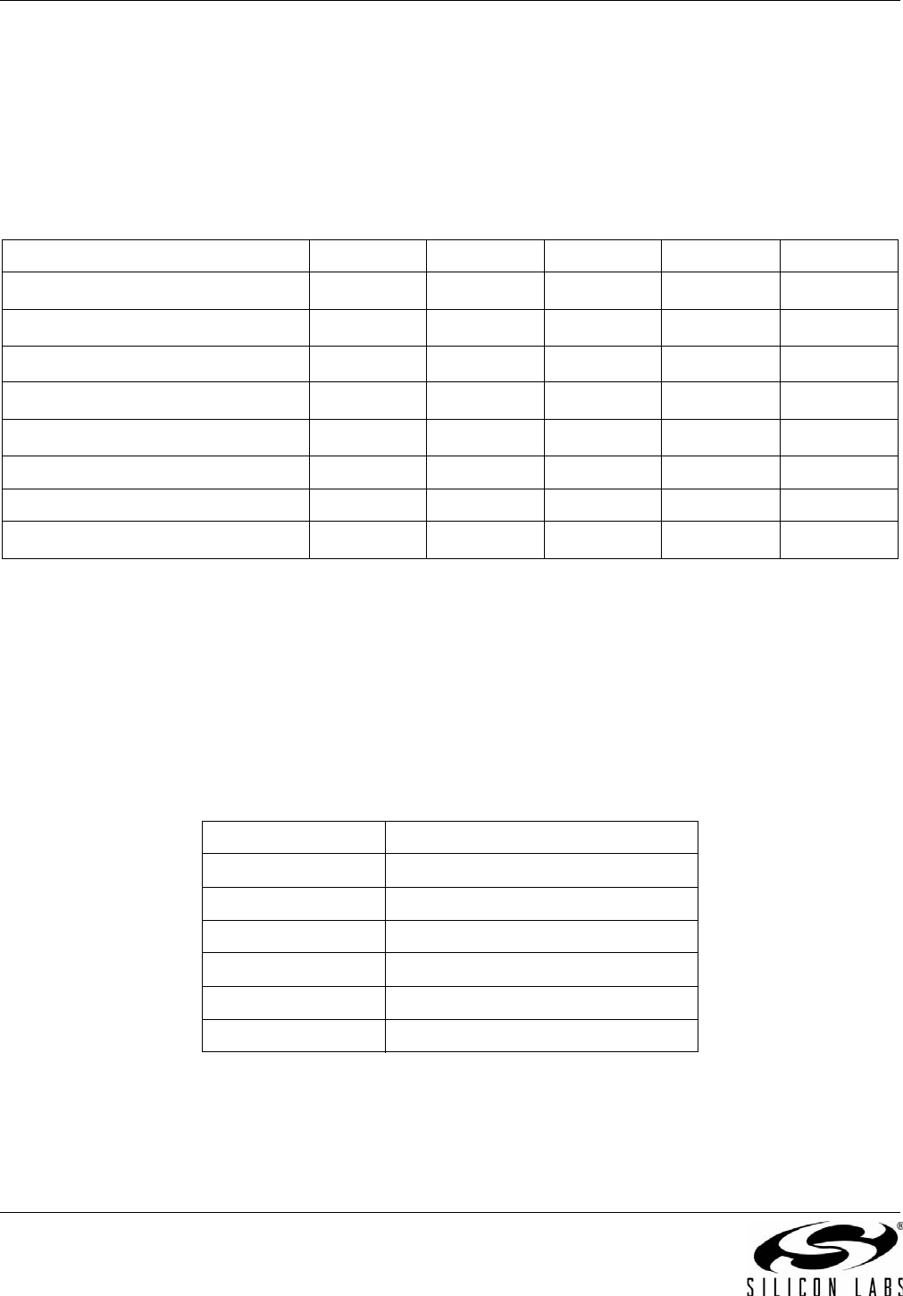
Table 12. Si5316, Si5322, Si5323, Si5365 and Si5366 Key Features
Si5316 Si5322 Si5323 Si5365 Si5366
SONET Frequencies
DATACOM Frequencies
DATACOM/SONET internetworking
Fixed Ratio between input clocks
Flexible Frequency Plan
Number of Inputs 2 2 2 4 4
Number of Outputs 1 2 2 5 5
Jitter Attenuation
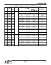
Table 13. Frequency Settings
FRQSEL[1:0] Output Frequency (MHz)
LL 19.38–22.28
LM 38.75–44.56
LH 77.50–89.13
ML 155.00–178.25
MM 310.00–356.50
MH 620.00–710.00