


Si53xx-RM
30 Rev. 0.5
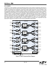
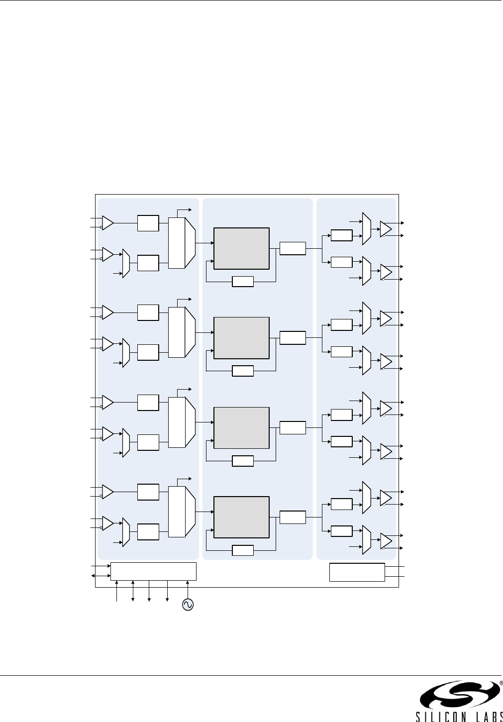
3.15. Si5374
The Si5374 is a highly integrated, 4-PLL jitter-attenuating precision clock multiplier for applications requiring sub 1
ps jitter performance. Each of the DSPLL® clock multiplier engines accepts two input clocks ranging from 2 kHz to
710 MHz and generates two independent, synchronous output clocks ranging from 2 kHz to 808 MHz. Each
DSPLL provides virtually any frequency translation across this operating range. For asynchronous, free-running
clock generation applications, the Si5374’s reference oscillator can be used as a clock source for the four DSPLLs.
The Si5374 input clock frequency and clock multiplication ratio are programmable through an I2C interface. The
Si5374 is based on Silicon Laboratories' 3rd-generation DSPLL® technology, which provides any-frequency
synthesis and jitter attenuation in a highly integrated PLL solution that eliminates the need for external VCXO and
loop filter components. Each DSPLL loop bandwidth is digitally programmable from 4 to 525 Hz, providing jitter
performance optimization at the application level. The device operates from a single 1.8 or 2.5 V supply with on-
chip voltage regulators with excellent PSRR. The Si5374 is ideal for providing clock multiplication and jitter
attenuation in high port count optical line cards requiring independent timing domains.
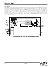
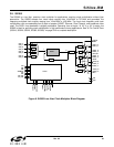
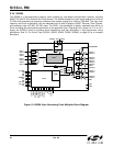
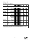
Figure 14. Si5374 Functional Block Diagram
CKIN3P_B
CKOUT3N_B
÷ N31
DSPLL
®
B
÷ NC1
÷ NC2
CKIN3N_B
CKIN4P_B
÷ N32
CKIN4N_B
Internal
Osc
PLL Bypass
CKOUT3P_B
CKOUT4N_B
CKOUT4P_B
f
OSC
÷ NC1_HS
Input
Monitor
Hitless
Switch
PLL Bypass
f
3
÷ N2
Status / Control
PLL Bypass
High PSRR
Voltage Regulator
VDD_q
GND
Synthesis Stage
CKIN1P_A
CKOUT1N_A
÷ N31
DSPLL
®
A
÷ NC1
÷ NC2
CKIN1N_A
CKIN2P_A
÷ N32
CKIN2N_A
Internal
Osc
PLL Bypass
CKOUT1P_A
CKOUT2N_A
CKOUT2P_A
Output Stage
f
OSC
÷ NC1_HS
Input
Monitor
Hitless
Switch
PLL Bypass
f
3
÷ N2
PLL Bypass
Input Stage
CKIN7P_D
CKOUT7N_D
÷ N31
DSPLL
®
D
÷ NC1
÷ NC2
CKIN7N_D
CKIN8P_D
÷ N32
CKIN8N_D
Internal
Osc
PLL Bypass
CKOUT7P_D
CKOUT8N_D
CKOUT8P_D
f
OSC
÷ NC1_HS
Input
Monitor
Hitless
Switch
PLL Bypass
f
3
÷ N2
PLL Bypass
CKIN5P_C
CKOUT5N_C
÷ N31
DSPLL
®
C
÷ NC1
÷ NC2
CKIN5N_C
CKIN6P_C
÷ N32
CKIN6N_C
Internal
Osc
PLL Bypass
CKOUT5P_C
CKOUT6N_C
CKOUT6P_C
f
OSC
÷ NC1_HS
Input
Monitor
Hitless
Switch
PLL Bypass
f
3
÷ N2
PLL Bypass
RSTL_q
CS_q
SCL SDA
LOL_q
IRQ_q
Low Jitter
XO or Clock
OSC_P/N