


Si53xx-RM
38 Rev. 0.5
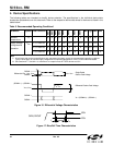
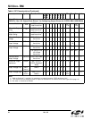
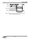
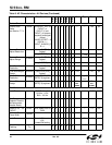
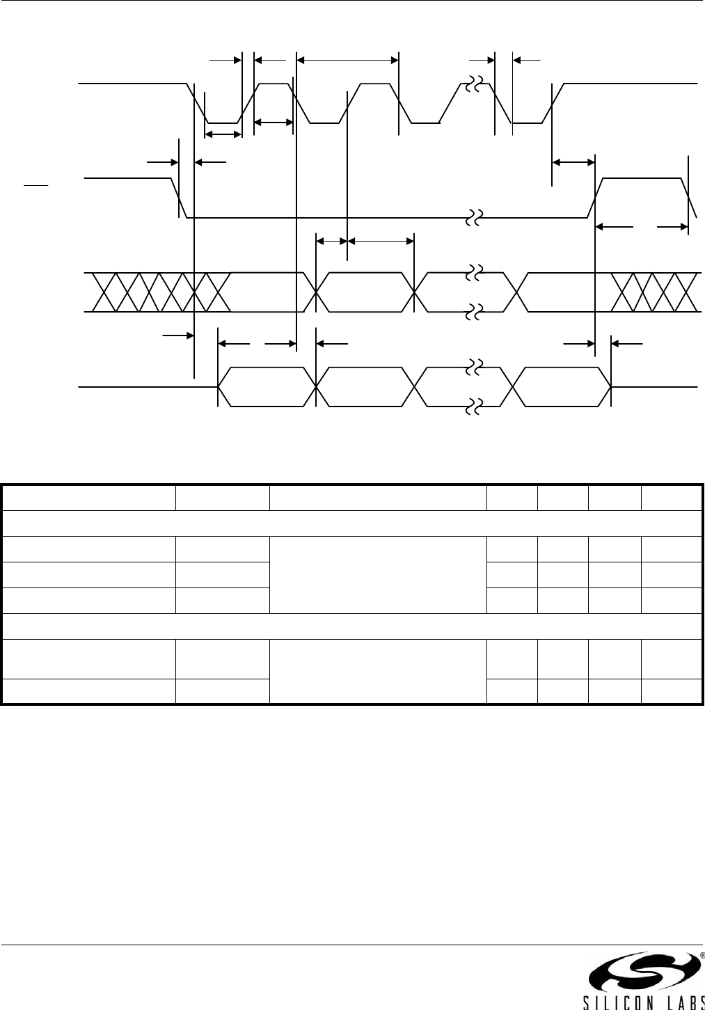
Figure 18. SPI Timing Diagram
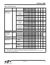
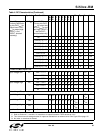
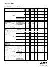
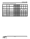
Table 7. DC Characteristics—Narrowband Devices (Si5316, Si5319, Si5323, Si5366, Si5368)
Parameter Symbol Test Condition Min Typ Max Unit
Single-Ended Reference Clock Input Pin XA (XB with cap to gnd)
Input Resistance XA
RIN
(RATE[1:0] = LM, ML, MH, or HM) — 10 — k
Input Voltage Level Limits XA
VIN
0—1.2 V
Input Voltage Swing XA
VPP
0.5 — 1.2 V
PP
Differential Reference Clock Input Pins (XA/XB)
Differential Input Voltage
Level Limits
XA/XB
VIN
(RATE[1:0] = LM, ML, MH, or HM) 0 — 1.2 V
Input Voltage Swing XA
VPP
/XB
VPP
0.5 — 2.4 V
PP
SCLK
SS
SDI
t
h1
t
d3
SDO
t
d1
t
d2
t
su1
t
r
t
f
t
c
t
su2
t
h2
t
cs
t
lsc
t
hsc