Si53xx-RM
Rev. 0.5 73
6.8. PLL Bypass Mode
The device supports a PLL bypass mode in which the selected input clock is fed directly to all enabled output
buffers, bypassing the DSPLL. In PLL bypass mode, the input and output clocks will be at the same frequency. PLL
bypass mode is useful in a laboratory environment to measure system performance with and without the effects of
jitter attenuation provided by the DSPLL.
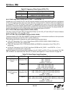
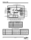
The DSBL2/BYPASS pin is used to select the PLL bypass mode according to Table 31.
Internally, the bypass path is implemented with high-speed differential signaling for low jitter. Bypass mode does
not support CMOS clock output.
6.9. Alarms
Summary alarms are available to indicate the overall status of the input signals and frame alignment (Si5366 only).
Alarm outputs stay high until all the alarm conditions for that alarm output are cleared.
6.9.1. Loss-of-Signal Alarms (Si5316, Si5322, Si5323, Si5365, Si5366)
The device has loss-of-signal circuitry that continuously monitors CKINn for missing pulses. The LOS circuitry
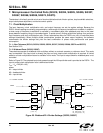
generates an internal LOSn_INT output signal that is processed with other alarms to generate CnB.
An LOS condition on CKIN1 causes the internal LOS1_INT alarm to become active. Similarly, an LOS condition on
CKINn causes the LOSn_INT alarm to become active. Once a LOSn_INT alarm is asserted on one of the input
clocks, it remains asserted until that input clock is validated over a designated time period. The time to clear
LOSn_INT after a valid input clock appears is listed in Table 8, “AC Characteristics—All Devices”. If another error
condition on the same input clock is detected during the validation time then the alarm remains asserted and the
validation time starts over.
6.9.1.1. Narrowband LOS Algorithm (Si5316, Si5323, Si5366)
The LOS circuitry divides down each input clock to produce an 8 kHz to 2 MHz signal. (For the Si5316, the output
of divider N3 (See Figure 1) is used.) The LOS circuitry over samples this divided down input clock using a 40 MHz
clock to search for extended periods of time without input clock transitions. If the LOS monitor detects twice the
normal number of samples without a clock edge, a LOSn_INT alarm is declared. Table 8, “AC Characteristics—All
Devices” gives the minimum and maximum amount of time for the LOS monitor to trigger.
6.9.1.2. Wideband LOS Algorithm (Si5322, Si5365)
Each input clock is divided down to produce a 78 kHz to 1.2 MHz signal before entering the LOS monitoring
circuitry. The same LOS algorithm as described in the above section is then used.
6.9.2. FOS Alarms (Si5365 and Si5366)
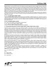
If FOS alarms are enabled (See Table 32), the internal frequency offset alarms (FOSn_INT) indicate if the input
clocks are within a specified frequency band relative to the frequency of CKIN2. The frequency offset monitoring
circuitry compares the frequency of the input clock(s) with CKIN2. If the frequency offset of an input clock exceeds
a preset frequency offset threshold, an FOS alarm (FOSn_INT) is declared for that clock input. Note that FOS
monitoring is not available on CKIN3 and CKIN4 if CK_CONF = 1. The device supports FOS hysteresis per GR-
1244-CORE, making the device less susceptible to FOS alarm chattering. A TCXO or OCXO reference clock must
be used in conjunction with either the SMC or Stratum 3/3E settings. Note that wander can cause false FOS
alarms.
Table 31. DSBL2/BYPASS Pin Settings
DSBL2/BYPASS Function
L CKOUT2 Enabled
M CKOUT2 Disabled
H PLL Bypass Mode w/ CKOUT2 Enabled


