


USB 2.0 Hi-Speed Hub Controller
Datasheet
SMSC USB251x 27 Revision 1.0 (3-11-09)
DATASHEET
5.3 Buffer Type Descriptions
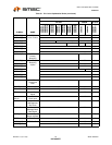
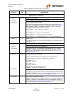
SEL48 I 48 MHz Clock Input Selection
48 MHz external input clock select. When the hub is clocked from an external
clock source, this pin selects either 24 MHz or 48 MHz mode.
‘0’ = 24 MHz
‘1’ = 48 MHz
POWER, GROUND, and NO CONNECTS
CRFILT VDD Core Regulator Filter Capacitor
This pin must have a 1.0 μF (or greater) ±20% (ESR <0.1 Ω) capacitor to
VSS.
VDD33 3.3 V Power
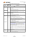
PLLFILT PLL Regulator Filter Capacitor
This pin must have a 1.0 μF (or greater) ±20% (ESR <0.1
Ω) capacitor to
VSS.
VSS Ground Pad / ePad
The package slug is the only VSS for the device and must be tied to ground
with multiple vias.
NC No Connect
No signal or trace should be routed or attached to these pins.
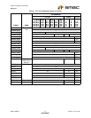
Table 5.3 Buffer Type Descriptions
BUFFER DESCRIPTION
I Input.
I/O Input/Output.
IPD Input with internal weak pull-down resistor.
IPU Input with internal weak pull-up resistor.
IS Input with Schmitt trigger.
O12 Output 12 mA.
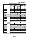
Table 5.2 USB251x Pin Descriptions (continued)
SYMBOL
BUFFER
TYPE DESCRIPTION