


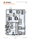
High Speed Inter-Chip USB 2.0 Hub and Flash Media Controller
Datasheet
Revision 1.0 (06-01-09) 16 SMSC USB4640/USB4640i
DATASHEET
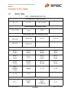
PRTCTL[3:2] 7
6
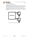
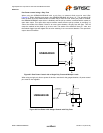
I/OD6PU USB Power Enable
As an output, these pins enable power to downstream USB
peripheral devices and have weak internal pull-up resistors. See
Section 6.3, "Port Power Control" for diagram and usage instructions.
As an input, when the power is enabled, these pins monitor the over-
current condition. When an over-current condition is detected, the
pins turn the power off.
RBIAS 47 I-R USB Transceiver Bias
A 12.0 k
Ω, ±1.0% resistor is attached from VSS to this pin in order
to set the transceiver's internal bias currents.
XTAL1 (CLKIN) 45 ICLKx 24 MHz Crystal Input or External Clock Input
This pin can be connected to one terminal of the crystal or it can be
connected to an external 24 MHz clock when a crystal is not used.
XTAL2 44 OCLKx 24 MHz Crystal Output
This is the other terminal of the crystal or it is left open when an
external clock source is used to drive XTAL1(CLKIN).
SECURE DIGITAL INTERFACE
SD_D[7:0] 19
20
23
30
32
33
17
18
I/O8PU Secure Digital Data 7-0
These are the bi-directional data signals SD_D0 - SD_D7 with weak
pull-up resistors.
SD_CLK 21 O8 Secure Digital Clock
This is an output clock signal to the SD/MMC device.
SD_CMD 24 I/O8PU Secure Digital Command
This is a bi-directional signal that connects to the CMD signal of the
SD/MMC device. The bi-directional signal has a weak internal pull-
up resistor.
GPIO15 /
SD_nCD
14 I/O6 This general purpose pin may be used either as input, edge sensitive
interrupt input, or output. Custom firmware is required to activate this
function.
I/O8PU Secure Digital Card Detect GPIO
This is a GPIO designated by the default firmware as the Secure
Digital card detection pin and has an internal pull-up.
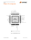
Table 6.1 USB4640/USB4640i Pin Descriptions (continued)
SYMBOL
48-PIN
QFN
BUFFER
TYPE
(Table 6.2)DESCRIPTION