


11
S93WD462/S93WD463
2029 2.2 1/23/01SUMMIT MICROELECTRONICS, Inc.
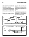
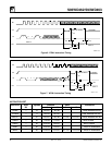
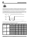
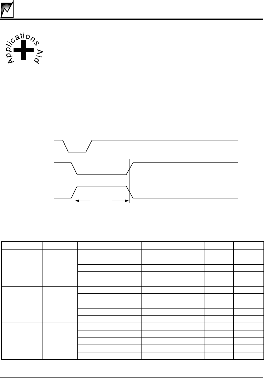
Frequently the reset controller will be deployed on a PC board that provides a peripheral function to a system.
Examples might be modem or network cards in a PC or a PCMCIA card in a laptop. In instances like this the peripheral
card may have a requirement for a clean reset function to insure proper operation. The system may or may not provide
a reset pulse of sufficient duration to clear the peripheral or to protect data stored in a nonvolatile memory.
The I/O capability of the RESET pins can provide a solution. The system’s reset signal to the peripheral can be fed
into the S93WD462/WD463 and it in turn can clean up the signal and provide a known entity to the peripheral’s circuits.
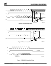
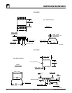
The figure below shows the basic timing characteristics under the assumption the reset input is shorter in duration
than t
PURST
. The same reset output affect can be attained by using the active high reset input.
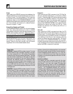
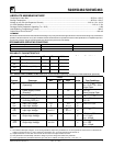
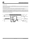
When planning your resistor pull-up and pull-down values, use the following chart to help determine min. resistances.
Condition Min Typ Max Units
V
CC
= 1.0V, I
OL
=100µA 0.3 V
V
CC
= 1.2V, I
OL
=100µA 0.3 V
V
CC
= 3.0V, I
OL
=500µA 0.3 V
V
CC
= 3.6V, I
OL
=500µA 0.3 V
V
CC
= 4.5V, I
OL
=750µA 0.3 V
V
CC
= 1.0V, I
OL
=100µA 0.4 V
V
CC
= 1.2V, I
OL
=150µA 0.4 V
V
CC
= 3.0V, I
OL
=750µA 0.4 V
V
CC
= 3.6V, I
OL
=1mA 0.4 V
V
CC
= 4.5V, I
OL
=1mA 0.4 V
V
CC
= 1.0V, I
OH
=400µA V
CC
-0.75 V
V
CC
= 1.2V, I
OH
=800µA V
CC
-0.75 V
V
CC
= 3.0V, I
OH
=800µA V
CC
-0.5 V
V
CC
= 3.6V, I
OH
=800µA V
CC
-0.5 V
V
CC
= 4.5V, I
OH
=800µA V
CC
-0.5 V
Worst Case RESET Sink/Source Capabilities at Various V
CC
Levels
Parameter Symbol
RESET# Output V
OL
Voltage
RESET# Output V
OL
Voltage
RESET Output V
OH
Voltage
2029 PGM T5.0
RESET#
Input
RESET#
Output
RESET
Output
2029 T fig09 2.0
t
PURST