


3
S93WD462/S93WD463
2029 2.2 1/23/01SUMMIT MICROELECTRONICS, Inc.
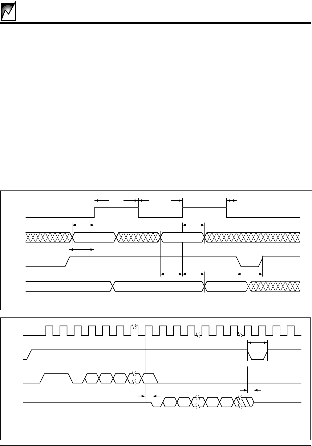
Instructions, addresses, and write data are clocked into
the DI pin on the rising edge of the clock (SK). The DO
pin is normally in a high impedance state except when
reading data from the device, or when checking the
ready/busy status after a write operation.
The ready/busy status can be determined after the start
of a write operation by selecting the device (CS high)
and polling the DO pin; DO low indicates that the write
operation is not completed, while DO high indicates that
the device is ready for the next instruction. See the
Applications Aid section for detailed use of the ready
busy status.
The format for all instructions is: one start bit; two op
code bits and either six (x16) or seven (x8) address or
instruction bits.
Read
Upon receiving a READ command and an address
(clocked into the DI pin), the DO pin of the S93WD462/
WD463 will come out of the high impedance state and,
will first output an initial dummy zero bit, then begin
shifting out the data addressed (MSB first). The output
data bits will toggle on the rising edge of the SK clock and
are stable after the specified time delay
(t
PD0
or t
PD1
).
Write
After receiving a WRITE command, address and the
data, the CS (Chip Select) pin must be deselected for a
minimum of 250ns (t
CSMIN
). The falling edge of CS will
start automatic erase and write cycle to the memory
location specified in the instruction. The ready/busy
status of the S93WD462/WD463 can be determined by
selecting the device and polling the DO pin.
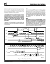
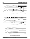
Figure 1. Sychronous Data Timing
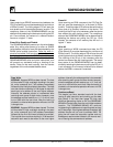
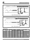
Figure 2. Read Instruction Timing
SK
2029 ILL 3.0
DI
CS
DO
t
DIS
t
PD0,
t
PD1
t
CSMIN
t
CSS
t
DIS
t
DIH
t
SKHI
t
CSH
VALID VALID
DATA VALID
t
SKLOW
SK
2029 ILL4.0
CS
DI
DO
t
CS
STANDBY
t
HZ
HIGH-ZHIGH-Z
11 0
A
N
A
N–1
A
0
0
D
N
D
N–1
D
1
D
0
t
PD0