2
S93WD462/S93WD463
2029 2.2 1/23/01
SUMMIT MICROELECTRONICS, Inc.
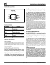
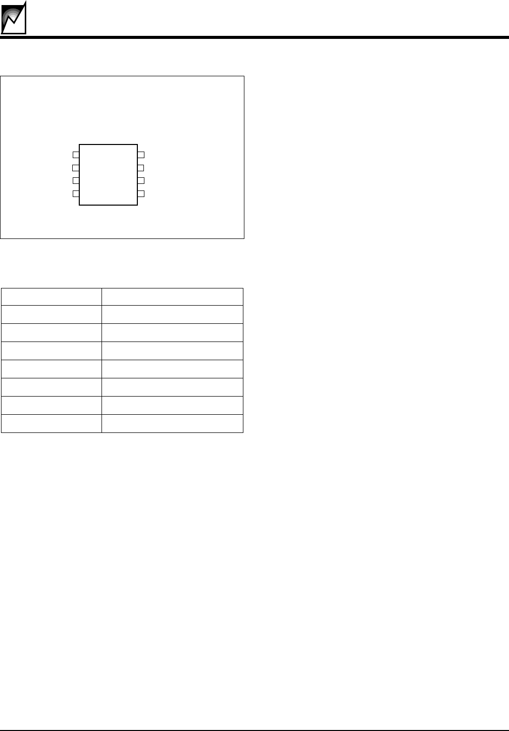
PIN FUNCTIONS
Pin Name Function
CS Chip Select
SK Clock Input
DI Serial Data Input
DO Serial Data Output
V
CC
+2.7 to 6.0V Power Supply
GND Ground
RESET/RESET# RESET I/O
PIN CONFIGURATION
DEVICE OPERATION
APPLICATIONS
The S93WD462/WD463 is ideal for applications requir-
ing low voltage and low power consumption. This device
provides microcontroller RESET control and can be
manually resettable.
RESET CONTROLLER DESCRIPTION
The S93WD462/WD463 provides a precision reset con-
troller that ensures correct system operation during
brownout and power-up/-down conditions. It is config-
ured with two open drain reset outputs; pin 7 is an active
high output and pin 6 is an active low output.
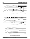
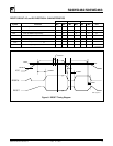
During power-up, the reset outputs remain active until
V
CC
reaches the V
TRIP
threshold. The outputs will con-
tinue to be driven for approximately 150ms after reaching
V
TRIP
. The reset outputs will be valid so long as V
CC
is ≥
1.0V. During power-down, the reset outputs will begin
driving active when V
CC
falls below V
TRIP
.
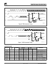
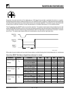
The reset pins are I/Os; therefore, the S93WD462/
WD463 can act as a signal conditioning circuit for an
externally applied reset. The inputs are edge triggered;
that is, the RESET input will initiate a reset time-out after
detecting a low to high transition and the RESET# input
will initiate a reset time-out after detecting a high to low
transition. Refer to the applications Information section
for more details on device operation as a debounce/
reset extender circuit.
It should be noted the reset outputs are open drain. When
used as outputs driving a circuit they need to be either
tied high (RESET#) or tied to ground (RESET) through
the use of pull-up or pull-down resistors. Refer to the
applications aid section for help in determining the value
of resistor to be used. Internally these pins are weakly
pulled up (RESET#) and pulled down (RESET): there-
fore, if the signals are not being used the pins may be left
unconnected.
WATCHDOG TIMER DESCRIPTION
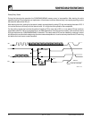
The S93WD462/WD463 has a watchdog timer with a
nominal time-out period of 1.6 seconds. Whenever the
watchdog times out, it will generate a reset output to both
pins 6 and 7. The watchdog timer is reset by any
transition on CS.
The watchdog timer will be held in a reset state during
power-on while V
CC
is less than V
TRIP
. Once V
CC
exceeds V
TRIP
the watchdog will continue to be held in
a reset state for the t
PURST
period. After t
PURST
it will be
released and the timer will begin operation. If either reset
input is asserted the watchdog timer will be reset and
remain in the reset condition until either t
PURST
has
expired or the reset input is released, whichever is
longer.
GENERAL OPERATION
The S93WD462/WD463 is a 1024-bit nonvolatile memory
intended for use with industry standard microproces-
sors. The S93WD463 is organized as X16, seven 9-bit
instructions control the reading, writing and erase
operations of the device. The S93WD462 is organized
as X8, seven 10-bit instructions control the reading,
writing and erase operations of the device. The device
operates on a single 3V or 5V supply and will generate on
chip, the high voltage required during any write opera-
tion.
CS
SK
DI
DO
V
CC
RESET
RESET#
GND
1
2
3
4
8
7
6
5
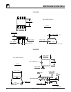
8-Pin PDIP
or 8-Pin SOIC
2029 T PCon 2.0


