


– 17 –
CXP854P60
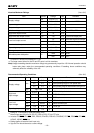
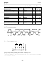
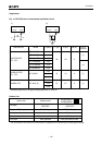
(7) OSD (On Screen Display) timing (Ta = –10 to +75°C, VDD = 4.5 to 5.5V, Vss = 0V)
Item
OSD clock frequency
HSYNC pulse width
HSYNC afterwrite
rise and fall times
VSYNC afterwrite
rise and fall times
fOSC
tHWD
tHCG
tVCG
EXLC
XLC
HSYNC
HSYNC
VSYNC
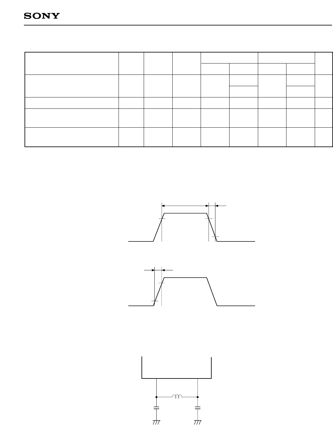
Fig. 12
Fig. 11
Fig. 11
Fig. 11
4
1.2
7
∗1
14
∗2
200
1.0
4
1.2
MHz
µs
ns
µs
11
∗1
16
∗2
200
1.0
Symbol Pin Condiiton Unit
Shadow Existent
Min. Max. Min. Max.
Shadow Non-existent
∗1
Oscillator clock at 4MHz operation
∗2
Oscillator clock at 8MHz operation
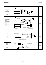
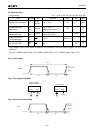
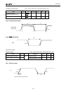
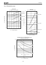
Fig. 11. OSD timing
0.8VDD
0.2VDD
tHCG
tHWD
HSYNC
For OPOL register (01FAH)
bit 7 at “0”
0.8VDD
0.2VDD
tVCG
VSYNC
For OPOL register (01FAH)
bit 6 at “0”
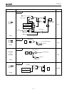
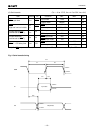
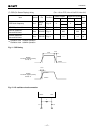
Fig. 12. LC oscillator circuit connection
L
C
2
C1
EXLC XLC