Chapter 3 – Electrical Characteristics
SocketModem Global MT5634SMI Developer’s Guide 15
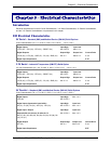
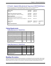
3.3V Parallel – Standard (SMI) and Industrial Temperature (SMI-ITP) Build Options
Electrical characteristics for Parallel MT5634SMI SocketModem devices are presented below.
3.3 Vdc Characteristics (TA = –40 °C to 85 °C; VDD = 3.3 V ± 0.3 V)
VDDMAX = 3.6 V
Digital Inputs
–DS (40)
Input High
Min 2.52 V
Input Low
Max 0.9 V
Digital Inputs (hysteresis input buffer)
A0 (31), A1 (25), A2 (34), –WR (32), –RD (33)
Input High
Min 2.52 V
Input Low
Max 0.9 V
Digital Input/Output
Output buffer can source 12 mA at 0.4 V
DO (37), D1 (38), D2 (29), D3 (39), D4 (35), D5 (36), D6
(41), D7 (27)
Input High
Min 2.52 V
Input Low
Max 0.9 V
Digital Output
INT (30)
Output High
Min 2.3 V
Output Low
Max 0.4 V
Current Drive
2 ma
Digital Input Capacitance 5 PF
Timing Requirements
Timing Requirements for Parallel Write
Parameter Min Max Unit
–DS to –WR Setup (low to low) 10 - ns
A0, A1, A2 to –WR Setup (valid to low) 15 - ns
–WR Pulse Width (low to high) 40 - ns
D0–D7 to –WR Setup (valid to high) 30 - ns
–WR to –DS hold (high to high) 0 - ns
–WR to A0–A2 Hold (high to invalid) 0 - ns
–WR to D0–D7 Hold (high to invalid) 0 - ns
–WR interaccess (high to low)
Non-MIMIC Accesses
MIMIC Accesses
10
110
-
-
ns
ns
Timing Requirements for Parallel Read
Parameter Min Max Unit
–DS to –RD Setup (low to low) 10 - ns
A0, A1, A2 to –RD Setup (valid to low) 15 - ns
–RD Pulse Width (low to high) 40 - ns
–RD to –DS hold (high to high) 0 - ns
–RD to A0–A2 Hold (high to invalid) 0 - ns
–WR interaccess (high to low)
Non-MIMIC Accesses
MIMIC Accesses
10
110
-
-
ns
ns
Handling Precautions
All MOS devices must be handled with certain precautions to avoid damage due to the accumulation of static charge.
Although input protection circuitry has been incorporated into the devices to minimize the effect of this static buildup,
proper precautions should be taken to avoid exposure to electrostatic discharge during handling and mounting.


