


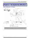

Chapter 4 – SocketModem Parallel Interface – A Programmer’s Description
SocketModem Global MT5634SMI Developer’s Guide 17
FIFO Operation
The 16-byte transmit and receive data FIFOs are enabled by the FIFO Control Register (FCR) bit-0. You can set
the receive trigger level via FCR bits 6/7. The receiver FIFO section includes a time-out function to ensure data is
delivered to the external host. An interrupt is generated whenever the Receive Holding Register (RHR) has not
been read following the loading of a character or the receive trigger level has been reached.
Receive (RX) FIFO
The RX FIFO can be configured to be 16 words deep and 11 bits wide. Each word in the RX FIFO consists of 8
data bits and 3 error bits. The RX block of the MMM contains read and write pointers and status flag circuitry
that need only to be presented with data (for input), reset, read/write control signals, and read/write clock signals.
The RX block of the MMM internally manages the FIFO register file and pointers, and it provides simultaneous
read/write capability (no contention problems).
The RX block of the MMM provides data (for output), FIFO full flag, FIFO empty flag, and an almost full flag
which uses an associated predefined trigger level (obtained from the MMM FCR control register) to signal when
the trigger level has been met. Four possible trigger levels may be selected by programming bits 6-7 of the FCR
control register.
A typical (interrupt driven) write to the RX block is a two-step process. The MMM micro-controller must first write
the 3 error bits to a shadow MMM LSR status register. Next, the micro-controller writes the data to the RX FIFO
and during this write operation, the 3 error bits are directly loaded from the LSR shadow register into the bits 8-
10 of the selected (11 bit-wide) FIFO register. These error bits represent the parity error, framing error, and break
interrupt signals associated with each data work transmission into the receive FIFO. When the receive FIFO is
read, these error bits are loaded directly into bits 2-4 of the MMM LSR register.
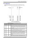
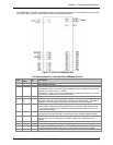
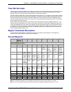
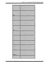
A2 A1 A0 Register Name Register Description Host Access
0
0
0
0
0
0
1
1
1
1
0
0
0
1
1
1
0
0
1
1
0
0
1
0
0
1
0
1
0
1
RBR
THR
IER
IIR
FCR
LCR
MCR
LSR
MSR
SCR
Receive Buffer (RX FIFO)
Transmit Holding (TX
FIFO)
Interrupt Enable
Interrupt Identification
FIFO Control
Line Control
Modem Control
Line Status
Modem Status
Scratch pad
DLAB = 0 R only
DLAB = 0 W only
DLAB = 0 R/W
DLAB = X R only
DLAB = X W only
DLAB = X R/W
DLAB = 0 R/W
DLAB = X R only
DLAB = X R only
DLAB = 0 R/W
0
0
1
1
0
0
1
0
0
1
1
0
DLL
DLM
DLX
MCX
LSB of Divisor Latch
MSB of Divisor Latch
Divisor Latch
Status/Control
DLAB = 1 R/W
DLAB = 1 R/W
DLAB = 1 R/W
DLAB = 1 R/W
Note 1* The General Register set is accessible only when DS is a logic 0.
Note 2* The Baud Rate register set is accessible only when DS is a logic 0 and LCR bit-7 is a logic 1.