


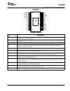

TPS54810
SLVS420B − MARCH 2002 − R EVISED FEBRUARY 2005
www.ti.com
13
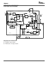
DETAILED DESCRIPTION
Under Voltage Lock Out (UVLO)
The TPS54810 incorporates an under voltage lockout
circuit to keep the device disabled when the input voltage
(VIN) is insufficient. During power up, internal circuits are
held inactive until VIN exceeds the nominal UVLO
threshold voltage of 3.80 V. Once the UVLO start threshold
is reached, device start-up begins. The device operates
until VIN falls below the nominal UVLO stop threshold of
3.5 V. Hysteresis in the UVLO comparator, and a 2.5-µs
rising and falling edge deglitch circuit reduce the likelihood
of shutting the device down due to noise on VIN.
Slow-Start/Enable (SS/ENA)
The slow-start/enable pin provides two functions. First, the
pin acts as an enable (shutdown) control by keeping the
device turned off until the voltage exceeds the start
threshold voltage of approximately 1.2 V. When SS/ENA
exceeds the enable threshold, device start up begins. The
reference voltage fed to the error amplifier is linearly
ramped up from 0 V to 0.891 V in 3.35 ms. Similarly, the
converter output voltage reaches regulation in
approximately 3.35 ms. Voltage hysteresis and a 2.5-µs
falling edge deglitch circuit reduce the likelihood of
triggering the enable due to noise.
The second function of the SS/ENA pin provides an
external means of extending the slow-start time with a
low-value capacitor connected between SS/ENA and
AGND.
Adding a capacitor to the SS/ENA pin has two effects on
start-up. First, a delay occurs between release of the
SS/ENA pin and start up of the output. The delay is
proportional to the slow-start capacitor value and lasts until
the SS/ENA pin reaches the enable threshold. The
start-up delay is approximately:
t
d
+ C
(SS)
1.2 V
5 mA
Second, as the output becomes active, a brief ramp-up at
the internal slow-start rate may be observed before the
externally set slow-start rate takes control and the output
rises at a rate proportional to the slow-start capacitor. The
ramp-up time set by the capacitor is approximately:
t
(d)
+ C
(SS)
0.7 V
5 mA
The actual ramp-up time is likely to be less than the above
approximation due to the brief ramp-up at the internal rate.
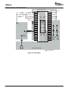
VBIAS Regulator (VBIAS)
The VBIAS regulator provides internal analog and digital
blocks with a stable supply voltage over variations in
junction temperature and input voltage. A high quality,
low-ESR, ceramic bypass capacitor is required on the
VBIAS pin. X7R or X5R grade dielectrics are
recommended because their values are more stable over
temperature. The bypass capacitor should be placed close
to the VBIAS pin and returned to AGND.
External loading on VBIAS is allowed, with the caution that
internal circuits require a minimum VBIAS of 2.70 V, and
external loads on VBIAS with ac or digital switching noise
may degrade performance. The VBIAS pin may be useful
as a reference voltage for external circuits.
Voltage Reference
The voltage reference system produces a precise V
ref
signal by scaling the output of a temperature stable
bandgap circuit. During manufacture, the bandgap and
scaling circuits are trimmed to produce 0.891 V at the
output of the error amplifier, with the amplifier connected
as a voltage follower. The trim procedure adds to the high
precision regulation of the TPS54810, since it cancels
offset errors in the scale and error amplifier circuits.
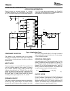
Oscillator and PWM Ramp
The oscillator frequency can be set to internally fixed
values of 350 kHz or 550 kHz using the SYNC pin as a
static digital input. If a different frequency of operation is
required for the application, the oscillator frequency can be
externally adjusted from 280 to 700 kHz by connecting a
resistor between the RT pin and AGND and floating the
SYNC pin. The switching frequency is approximated by
the following equation, where R is the resistance from RT
to AGND:
Switching Frequency +
100 kW
R
500 [kHz]
External synchronization of the PWM ramp is possible
over the frequency range of 330 kHz to 700 kHz by driving
a synchronization signal into SYNC and connecting a
resistor from RT to AGND. Choose an RT resistor which
sets the free running frequency to 80% of the
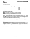
synchronization signal. The following table summarizes
the frequency selection configurations:
SWITCHING FRE-
QUENCY
SYNC PIN RT PIN
350 kHz, internally set Float or AGND Float
550 kHz, internally set =2.5 V Float
Externally set 280 kHz
to 700 kHz
Float R = 68 k to 180 k
Externally synchro-
nized frequency
Synchronization
signal
R = RT value for 85%
of external synchro-
nization frequency
Error Amplifier
The high performance, wide bandwidth, voltage error
amplifier sets the TPS54810 apart from most dc/dc
converters. The user is given the flexibility to use a wide
range of output L and C filter components to suit the
(2)
(3)
(4)