


TPS54810
SLVS420B − MARCH 2002 − R EVISED FEBRUARY 2005
www.ti.com
9
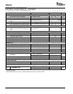
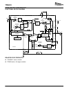
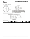
PCB LAYOUT
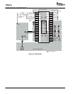
Figure 10 shows a generalized PCB layout guide for the
TPS54810
The VIN pins are connected together on the printed-circuit
board (PCB) and bypassed with a low-ESR
ceramic-bypass capacitor. Care should be taken to
minimize the loop area formed by the bypass capacitor
connections, the VIN pins, and the TPS54810 ground
pins. The minimum recommended bypass capacitance is
10-µF ceramic capacitor with a X5R or X7R dielectric and
the optimum placement is closest to the VIN pins and the
PGND pins.
The TPS54810 has two internal grounds (analog and
power). Inside the TPS54810, the analog ground ties to all
of the noise sensitive signals, while the power ground ties
to the noisier power signals. Noise injected between the
two grounds can degrade the performance of the
TPS54810, particularly at higher output currents. Ground
noise on an analog ground plane can also cause problems
with some of the control and bias signals. For these
reasons, separate analog and power ground traces are
recommended. There is an area of ground on the top layer
directly under the IC, with an exposed area for connection
to the PowerPAD. Use vias to connect this ground area to
any internal ground planes. Additional vias are also used
at the ground side of the input and output filter capacitors.
The AGND and PGND pins are tied to the PCB ground by
connecting them to the ground area under the device as
shown. The only components that tie directly to the power
ground plane are the input capacitors, the output
capacitors, the input voltage decoupling capacitor, and the
PGND pins of the TPS54810. Use a separate wide trace
for the analog ground signal path. The analog ground is
used for the voltage set point divider, timing resistor RT,
slow-start capacitor and bias capacitor grounds. Connect
this trace directly to AGND (Pin 1).
The PH pins are tied together and routed to the output
inductor. Since the PH connection is the switching node,
the inductor is located close to the PH pins. The area of the
PCB conductor is minimized to prevent excessive
capacitive coupling.
Connect the boot capacitor between the phase node and
the BOOT pin as shown Keep the boot capacitor close to
the IC and minimize the conductor trace lengths.
Connect the output filter capacitor(s) as shown between
the VOUT trace and PGND. It is important to keep the loop
formed by the PH pins, L
OUT
, C
OUT
and PGND as small as
practical.
Place the compensation components from the VOUT trace
to the VSENSE and COMP pins. Do not place these
components too close to the PH trace. Due to the size of
the IC package and the device pin-out, they must be routed
close, but maintain as much separation as possible while
still keeping the layout compact.
Connect the bias capacitor from the VBIAS pin to analog
ground using the isolated analog ground trace. If a
slow-start capacitor or RT resistor is used, or if the SYNC
pin is used to select 350-kHz operating frequency, connect
them to this trace.