


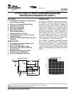
TPS54810
SLVS420B − MARCH 2002 − R EVISED FEBRUARY 2005
www.ti.com
2
These devices have limited built-in ESD protection. The leads should be shorted together or the device placed in conductive foam during
storage or handling to prevent electrostatic damage to the MOS gates.
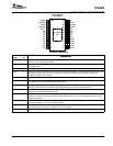
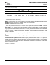
ORDERING INFORMATION
T
A
OUTPUT VOLTAGE PACKAGE PART NUMBER
−40°C to 85°C 0.9 V to 3.3 V PLASTIC HTSSOP (PWP)
(1)
TPS54810PWP
(1)
The PWP package is also available taped and reeled. Add an R suffix to the device type (i.e., TPS54810PWPR). See the application section
of the data sheet for PowerPAD™ drawing and layout information.
(2)
For the most current package and ordering information, see the Package Option Addendum at the end of this document, or see the TI website
at www.ti.com.
ABSOLUTE MAXIMUM RATINGS
over operating free-air temperature range unless otherwise noted
(1)
TPS54810 UNIT
VIN, SS/ENA, SYNC −0.3 to 7
I t lta a V
RT −0.3 to 6
V
Input voltage range, V
I
VSENSE −0.3 to 4
V
BOOT −0.3 to 17
O t t lta a V
VBIAS, COMP, PWRGD −0.3 to 7
V
Output voltage range, V
O
PH −0.6 to 10
V
S t I
PH Internally Limited
Source current, I
O
COMP, VBIAS 6 mA
PH 12 A
Sink current, I
S
COMP 6
A
Sink current, I
S
SS/ENA, PWRGD 10
mA
Voltage differential AGND to PGND ±0.3 V
Operating virtual junction temperature range, T
J
−40 to 125 °C
Storage temperature, T
stg
−65 to 150 °C
Lead temperature 1,6 mm (1/16 inch) from case for 10 seconds 300 °C
(1)
Stresses beyond those listed under “absolute maximum ratings” may cause permanent damage to the device. These are stress ratings only, and
functional operation of the device at these or any other conditions beyond those indicated under “recommended operating conditions” is not
implied. Exposure to absolute-maximum-rated conditions for extended periods may affect device reliability.
RECOMMENDED OPERATING CONDITIONS
MIN NOM MAX UNIT
Input voltage range, V
I
4 6 V
Operating junction temperature, T
J
−40 125 °C
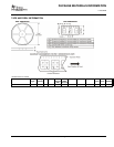
DISSIPATION RATINGS
(1)
(2)
PACKAGE
THERMAL IMPEDANCE
JUNCTION-TO-AMBIENT
T
A
≤ 25°C
POWER RATING
T
A
= 70°C
POWER RATING
T
A
= 85°C
POWER RATING
28-Pin PWP with solder 18.2 °C/W 5.49 W
(2)
3.02 W 2.20 W
28-Pin PWP without solder 40.5 °C/W 2.48 W 1.36 W 0.99 W
(1)
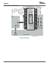
For more information on the PWP package, refer to TI technical brief, literature number SLMA002.
(2)
Test Board Conditions:
1. 3” x 3”, 4 layers, thickness: 0.062”
2. 1.5 oz. copper traces located on the top of the PCB
3. 1.5 oz. copper ground plane on the bottom of the PCB
4. 0.5 oz. copper ground planes on the 2 internal layers
5. 12 thermal vias (see “Recommended Land Pattern” in applications section of this data sheet)
(3)
Maximum power dissipation may be limited by over current protection.