


TPS54810
SLVS420B − MARCH 2002 − R EVISED FEBRUARY 2005
www.ti.com
5
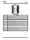
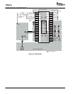
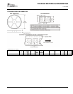
1
2
3
4
5
6
7
8
9
10
11
12
13
14
28
27
26
25
24
23
22
21
20
19
18
17
16
15
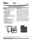
AGND
VSENSE
COMP
PWRGD
BOOT
PH
PH
PH
PH
PH
PH
PH
PH
PH
RT
SYNC
SS/ENA
VBIAS
VIN
VIN
VIN
VIN
VIN
PGND
PGND
PGND
PGND
PGND
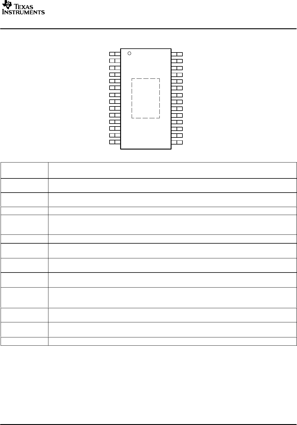
PWP PACKAGE
(TOP VIEW)
THERMAL
PAD
Terminal Functions
TERMINAL
DESCRIPTION
NAME NO.
DESCRIPTION
AGND 1 Analog ground. Return for compensation network/output divider, slow-start capacitor, VBIAS capacitor, RT resistor and
SYNC pin. Connect PowerPAD to AGND.
BOOT 5 Bootstrap input. 0.022-µF to 0.1-µF low-ESR capacitor connected from BOOT to PH generates floating drive for the
high-side FET driver.
COMP 3 Error amplifier output. Connect frequency compensation network from COMP to VSENSE.
PGND 15−19 Power ground. High current return for the low-side driver and power MOSFET. Connect PGND with large copper areas
to the input and output supply returns, and negative terminals of the input and output capacitors. A single point
connection to AGND is recommended.
PH 6−14 Phase input/output. Junction of the internal high-side and low-side power MOSFETs, and output inductor.
PWRGD 4 Power good open drain output. High-Z when VSENSE ≥ 90% V
ref
, otherwise PWRGD is low. Note that output is low
when SS/ENA is low or the internal shutdown signal is active.
RT 28 Frequency setting resistor input. Connect a resistor from RT to AGND to set the switching frequency. When using the
SYNC pin, set the RT value for a frequency at or slightly lower than the external oscillator frequency.
SS/ENA 26 Slow-start/enable input/output. Dual function pin which provides logic input to enable/disable device operation and
capacitor input to externally set the start-up time.
SYNC 27 Synchronization input. Dual function pin which provides logic input to synchronize to an external oscillator or pin select
between two internally set switching frequencies. When used to synchronize to an external signal, a resistor must be
connected to the RT pin.
VBIAS 25 Internal bias regulator output. Supplies regulated voltage to internal circuitry. Bypass VBIAS pin to AGND pin with a
high quality, low-ESR 0.1-µF to 1.0-µF ceramic capacitor.
VIN
20−24 Input supply for the power MOSFET switches and internal bias regulator. Bypass VIN pins to PGND pins close to
device package with a high quality, low-ESR 10-µF ceramic capacitor.
VSENSE 2 Error amplifier inverting input. Connect to output voltage through compensation network/output divider.