


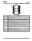
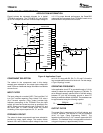
TPS54810
SLVS420B − MARCH 2002 − R EVISED FEBRUARY 2005
www.ti.com
4
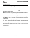
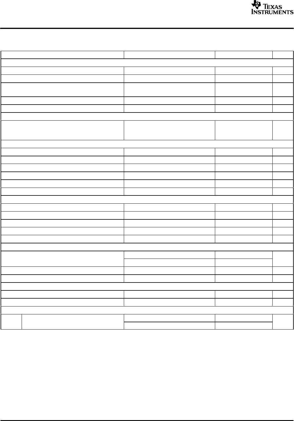
ELECTRICAL CHARACTERISTICS CONTINUED
T
J
= −40°C to 125°C, V
I
= 4 V to 6 V unless otherwise noted
PARAMETER TEST CONDITIONS MIN TYP MAX UNIT
ERROR AMPLIFIER
Error amplifier open loop voltage gain 1 kΩ COMP to AGND
(1)
90 110 dB
Error amplifier unity gain bandwidth Parallel 10 kΩ, 160 pF COMP to AGND
(1)
3 5 MHz
Error amplifier common mode input voltage
range
Powered by internal LDO
(1)
0 VBIAS V
Input bias current, VSENSE VSENSE = V
ref
60 250 nA
Output voltage slew rate (symmetric), COMP 1.0 1.4 V/µs
PWM COMPARATOR
PWM comparator propagation delay time, PWM
comparator input to PH pin (excluding dead-
time)
10-mV overdrive
(1)
70 85 ns
SLOW-START/ENABLE
Enable threshold voltage, SS/ENA 0.82 1.20 1.40 V
Enable hysteresis voltage, SS/ENA
(1)
0.03 V
Falling edge deglitch, SS/ENA
(1)
2.5 µs
Internal slow-start time 2.6 3.35 4.1 ms
Charge current, SS/ENA SS/ENA = 0V 3 5 8 µA
Discharge current, SS/ENA SS/ENA = 1.3 V, V
I
= 1.5 V 1.5 2.3 4.0 mA
POWER GOOD
Power good threshold voltage VSENSE falling 90 %V
ref
Power good hysteresis voltage
(1)
3 %V
ref
Power good falling edge deglitch
(1)
35 µs
Output saturation voltage, PWRGD I
(sink)
= 2.5 mA 0.18 0.3 V
Leakage current, PWRGD V
I
= 3.6 V 1 µA
CURRENT LIMIT
Current limit
V
I
= 4.5 V
(1)
, output shorted 9 11
A
Current limit
V
I
= 6 V
(1)
, output shorted 10 12
A
Current limit leading edge blanking time 100 ns
Current limit total response time 200 ns
THERMAL SHUTDOWN
Thermal shutdown trip point
(1)
135 150 165 _C
Thermal shutdown hysteresis
(1)
10 _C
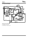
OUTPUT POWER MOSFETS
P MOSFET it h
V
I
= 6 V
(2)
26 47
Ω
r
DS(on)
Power MOSFET switches
V
I
= 4.5 V
(2)
30 60
mΩ
(1)
Specified by design
(2)
Matched MOSFETs, low-side r
DS(on)
production tested, high-side r
DS(on)
production tested.