


[6] Handling Guide
104
3.3.11 Latch-up
CMOS devices are subject to latch-up, an undesirable condition in which a parasitic PNPN junction
(thyristor) in the CMOS IC conducts. An abnormal current of several hundred mA can flow between
V
CC
and GND, destroying the IC.
Latch-up occurs when the voltage applied to the input or output pins exceeds the prescribed
absolute maximum rating value, causing a large current to flow in the device, or when the V
CC
pin
voltage exceeds (even momentarily) the absolute maximum rating value causing internal components
to break down. Latch-up results in a large, continuous current between V
CC
and GND and can cause
overheating and burn-out. To avoid this, observe the following precautions.
(1) Ensure that the voltage level on the input/output pins is no higher than V
CC
and no lower than
V
SS
, taking into account the timing at power-on. (As the V
CC
and V
SS
levels vary from device to
device, please refer to the datasheet for the device in question.)
(2) Do not subject the device to abnormal noise.
(3) Fix the potential of any unused input pins to V
CC
or V
SS
.
(4) Do not connect output pins directly to other output pins, or to V
CC
or VSS.
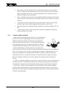
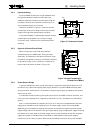
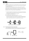
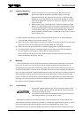
Since ample margin against latch-up is provided, there is no problem if Min-CMOS devices are
used within their specifications. However, since the interface component may receive excessive
surges, it is recommended that protective circuits be added, as shown in Figure 3.5.
Figure 3.5 Example of Latch-up Prevention Methods
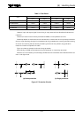
3.3.12 Electrical Discharge and Precautions against Noise
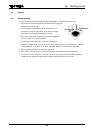
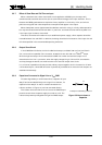
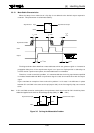
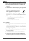
The Mini-MOS Series have ample margin for handling noise such as electrical discharge. Figure 3.6
show a circuit for ESD testing and Table 3.1 shows the results of ESD tests for various devices.
Figure 3.6 Test Circuit
I/O
R
I/O
I/O
R
R
A
s
EIAJ Method : C = 200 pF
R = 0 Ω
MIL-STD Method : C = 100 pF
C = 1.5 kΩ
Input
or
Output
V
CC
, GND