


[6] Handling Guide
110
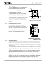
3.4.2 Inspection Sequence
1. Do not insert devices in the wrong orientation. Make sure that the
positive and negative electrodes of the power supply are correctly
connected. Otherwise, the rated maximum current or maximum power
dissipation may be exceeded and the device may break down or undergo
performance degradation, causing it to catch fire or explode, resulting in
injury to the user.
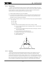
2. When conducting any kind of evaluation, inspection or testing using AC
power with a peak voltage of 42.4 V or DC power exceeding 60 V, be sure
to connect the electrodes or probes of the testing equipment to the device
under test before powering it on. Connecting the electrodes or probes of
testing equipment to a device while it is powered on may result in electric
shock, causing injury.
(1) Apply voltage to the test jig only after inserting the device securely into it. When applying or
removing power, observe the relevant precautions, if any.
(2) Make sure that the voltage applied to the device is off before removing the device from the test jig.
Otherwise, the device may undergo performance degradation or be destroyed.
(3) Make sure that no surge voltages from the measuring equipment are applied to the device.
(4) The chips housed in tape carrier packages (TCPs) are bare chips and are therefore exposed.
During inspection take care not to crack the chip or cause any flaws in it.
Electrical contact may also cause a chip to become faulty. Therefore make sure that nothing
comes into electrical contact with the chip.
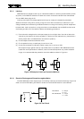
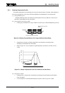
3.5 Mounting
There are essentially two main types of semiconductor device package: lead insertion and surface
mount. During mounting on printed circuit boards, devices can become contaminated by flux or
damaged by thermal stress from the soldering process. With surface-mount devices in particular, the
most significant problem is thermal stress from solder reflow, when the entire package is subjected to
heat. This section describes a recommended temperature profile for each mounting method, as well as
general precautions which you should take when mounting devices on printed circuit boards. Note,
however, that even for devices with the same package type, the appropriate mounting method varies
according to the size of the chip and the size and shape of the lead frame. Therefore, please consult
the relevant technical datasheet and databook.
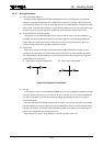
3.5.1 Lead Forming
1. Always wear protective glasses when cutting the leads of a device with
clippers or a similar tool. If you do not, small bits of metal flying off the
cut ends may damage your eyes.
2. Do not touch the tips of device leads. Because some types of device have
leads with pointed tips, you may prick your finger.
Semiconductor devices must undergo a process in which the leads are cut and formed before the
devices can be mounted on a printed circuit board. If undue stress is applied to the interior of a device
during this process, mechanical breakdown or performance degradation can result. This is
attributable primarily to differences between the stress on the device’s external leads and the stress