


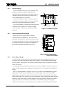

[6] Handling Guide
105
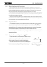
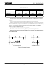
Table 3.1 Test Result
EIAJ Method MIL-STD Method
Name
Input Output Input Output
TC7MH244FK >±200 V >±200 V >±2000 V >±2000 V
TC7MET244AFK >±200 V >±200 V >±2000 V >±2000 V
TC7MZ244FK >±200 V >±200 V >±2000 V >±2000 V
TC7MA244FK >±200 V >±200 V >±2000 V >±2000 V
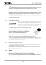
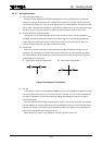
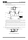
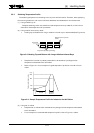
However, input and output signal lines are long in many cases and have distributed inductance or
reactance.
Therefore, if these lines are directly connected to CMOS, various problems can arise.
Possible problems are malfunction due to induced noise, or destruction of the input/output elements
due to a surge. Reducing the signal line impedance (driving impedance) or inserting noise-eliminating
circuits on the receiving side are two ways of dealing with the former problem; surge protection
measures are taken to cope with the latter.
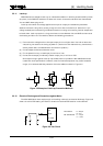
Figure 3.7 shows an example of noise and surge protection.
Alternatively, the PCB can be isolated using a photocoupler or a lead relay connection.
Note that it is not necessary to make design allowances for the overshoot and undershoot which can
occur under light loads.
(a) Noise protection (b) Surge protection
Figure 3.7 Protection Circuits