


TC9457F
2002-10-21
12
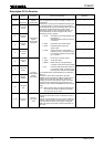
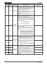
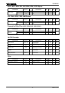
I/O Ports
(P1-0 to P4-3)
Characteristics Symbol
Test
Circuit
Test Condition Min Typ. Max Unit
High level I
OH3
― V
OH
= 4.5 V −1 −2 ―
I
OL3
―
V
OL
= 0.5 V
(exclude P4-1, 2, 3 pin)
1.5 3.0 ―
Output current
Low level
I
OL5
― V
OL
= 0.5 V (P4-1, 2, 3 pin) 4 10 ―
mA
Input leakage current I
LI
― V
IH
= 5.0 V, V
IL
= 0 V ― ― ±1.0 µA
High level V
IH
― ―
MV
DD
× 0.8
~ MV
DD
Input voltage
Low level V
IL
― ― 0 ~
MV
DD
× 0.2
V
Input pullup/down resistance R
IN1
―
(P1-0 to P1-3) When pulldown,
pullup are set.
25 50 120 kΩ
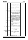
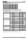
HOLD
, INTR Input Port,
RESET
Input
Characteristics Symbol
Test
Circuit
Test Condition Min Typ. Max Unit
Input leakage current I
LI
― V
IH
= 5.0 V, V
IL
= 0 V ― ― ±1.0 µA
High level V
IH3
― ―
MV
DD
× 0.8
~ MV
DD
Input voltage
Low level V
IL3
― ― 0 ~
MV
DD
× 0.2
V
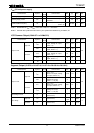
A/D Converter
(AD
IN1
to AD
IN4
)
Characteristics Symbol
Test
Circuit
Test Condition Min Typ. Max Unit
Analog input voltage range V
AD
― AD
IN
to AD
IN4
0 ~ MV
DD
V
Resolution V
RES
― ― ― 6 ― bit
Overall conversion error ― ― ― ― ±0.5 ±4.0 LSB
Analog input leakage I
LI
―
V
IH
= 5.0 V, V
IL
= 0 V
(AD
IN1
to AD
IN4
)
― ― ±1.0 µA
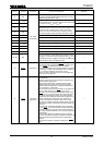
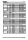
DATA, SFSY, LRCK, BCK, AOUT, MBOV, IPF Outputs and CLCK Input/Output
Characteristics Symbol
Test
Circuit
Test Condition Min Typ. Max Unit
High level I
OH4
―
V
OH
= 4.5 V
(Settings OT for output,
LEDon = 0)
−2.0 −4.0 ―
Output current
Low level I
OL5
―
V
OL
= 0.5 V
(Settings OT for output,
LEDon = 0)
5 10 ―
mA
Input leakage current I
LI
―
V
IH
= 5.0 V, V
IL
= 0 V
(CLCK)
― ― ±1.0 µA
High level V
IH
― (CLCK)
MV
DD
× 0.8
~ MV
DD
Input voltage
Low level V
IL
― (CLCK) 0 ~
MV
DD
× 0.2
V