


TC9457F
2002-10-21
5
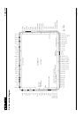
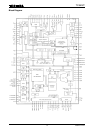
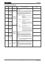
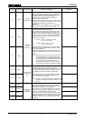
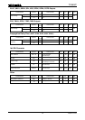
Description Of Pin Function
Pin No. Symbol Pin Name Function And Operation Remarks
1~10
S1/OT5
~
S10/OT14
LCD segment
outputs
/Output ports
―
11
S11/OT15
/CLCK
―
12
S12/OT16
/DATA
―
13
S13/OT17
/SFSY
―
14
S14/OT18
/LRCK
LCD segment
outputs
/Output ports
/CD signals
―
15
S8-0/S15
/BCK
―
16
P8-1/S16
/AOUT
―
17
P8-2/S17
/MBOV
―
18
P8-3/S18
/IPF
I/O ports
/LCD segment
outputs
/CD signals
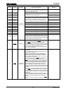
Segment signal outputs to the LCD panel.
Up to 72 segments in a matrix with COM1 to COM4 can
be displayed.
All of the S1 to S18 pins can be switched for output ports
by a program (Note 1). Also, the S15 to S18 pins each
can be switched for I/O ports individually. When set for I/O
ports, these pins become Nch open-drain outputs.
Furthermore, the S11 to S14 and the P8-0 to P8-3 pins
can be switched for use as CD signal (CLCK to IPF)
input/output pins by a program.
· CLCK : Subcodes P thru W data readout clock
input/output.
Selected between input and output by
a command.
· DATA : Subcodes P thru W data output.
· SFSY : Playback system frame sync
signal output.
· LRCK : Channel clock (44.1 kHz) output. It
outputs a low for L channel and a high
for R channel. Polarity can be inverted
by a command.
· BCK : Bit clock (1,4112 MHz) output.
· AOUT : Audio data output.
· MBOV : Buffer memory-over signal output.
It outputs a high when buffer overflows.
· IPF : Correction flag output. When AOUT is
C2 correction output, it outputs a high
indicating that
correction is impossible.
For CD signal output, set parameters OT for output and
LEDon = 1.
Furthermore, when set for output ports, the buffer
capability can be increased by setting the LEDon bit to 1,
so that it can be used as an LED driver. These pins
normally are used for LED segment outputs.
Since the
output ports can increment OT1 through OT18 by an
instruction, data in external RAM/ROM can be accessed
easily.
Note 1: After a system reset, the output port shared pins
are set for LCD output and the I/O port shared
pins are set for I/O port input.
―
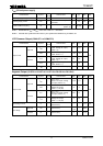
21~24
P1-0~P1-3
/K0~K3
I/O port 1
/Key input
ports
4-bit CMOS I/O ports.
These ports can be set for input or output bit for bit by a
program.
These pins can be pulled up to V
DD
or down to GND by a
program. Therefore, they can be used as key input pins.
Also, when they are set for I/O port input, a change of
state in this input can be used to clear the clock stop or
wait mode.
―