


0
PLB PCI Full Bridge (v1.00a)
DS508 March 21, 2006
0 0
Product Specification
DS508 March 21, 2006 www.xilinx.com 1
Product Specification
© 2005 Xilinx, Inc. All rights reserved. All Xilinx trademarks, registered trademarks, patents, and further disclaimers are as listed at http://www.xilinx.com/legal.htm. All other trademarks and
registered trademarks are the property of their respective owners. All specifications are subject to change without notice.
NOTICE OF DISCLAIMER: Xilinx is providing this design, code, or information "as is." By providing the design, code, or information as one possible implementation of this feature, application,
or standard, Xilinx makes no representation that this implementation is free from any claims of infringement. You are responsible for obtaining any rights you may require for your implemen-
tation. Xilinx expressly disclaims any warranty whatsoever with respect to the adequacy of the implementation, including but not limited to any warranties or representations that this imple-
mentation is free from claims of infringement and any implied warranties of merchantability or fitness for a particular purpose.
E
A
RLY AC
C
ESS
Introduction
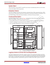
The PLB PCI Full Bridge design provides full bridge
functionality between the Xilinx 64-bit PLB and a 32-bit
Revision 2.2 compliant Peripheral Component
Interconnect (PCI) bus. The bridge is referred to as the
PLB PCI Bridge in this document.
The Xilinx PLB is a 64-bit bus subset of the IBM PLB
described in the 64-Bit Processor Local Bus Architecture
Specification v3.5. Details on the Xilinx PLB and the PLB
IPIF are found in the Processor IP Reference Guide. This
guide is accessed via EDK help or the Xilinx website at:
http://www.xilinx.com/ise/embedded/proc_ip_ref_
guide.pdf.
The LogiCORE PCI v3.0 core provides an interface with
the PCI bus. Details of the LogiCORE PCI 32 v3.0 core
operation is found in the
Xilinx LogiCORE PCI Interface
v3.0 Product Specification and the Xilinx The Real-PCI
Design Guide v3.0.
Host bridge functionality (often called North bridge
functionality) is an optional functionality.
Configuration Read and Write PCI commands can be
performed from the PLB-side of the bridge. The PLB
PCI Bridge supports a 32-bit/33 MHz PCI bus only.
Exceptions to the support of PCI commands supported
by the v3.0 core are outlined in the
Features section.
The PLB PCI Bridge design has parameters that allow
customers to configure the bridge to suit their
application. The parameterizable features of the design
are discussed in the
Bus Interface Parameters section.
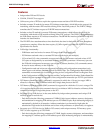
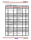
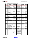
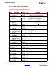
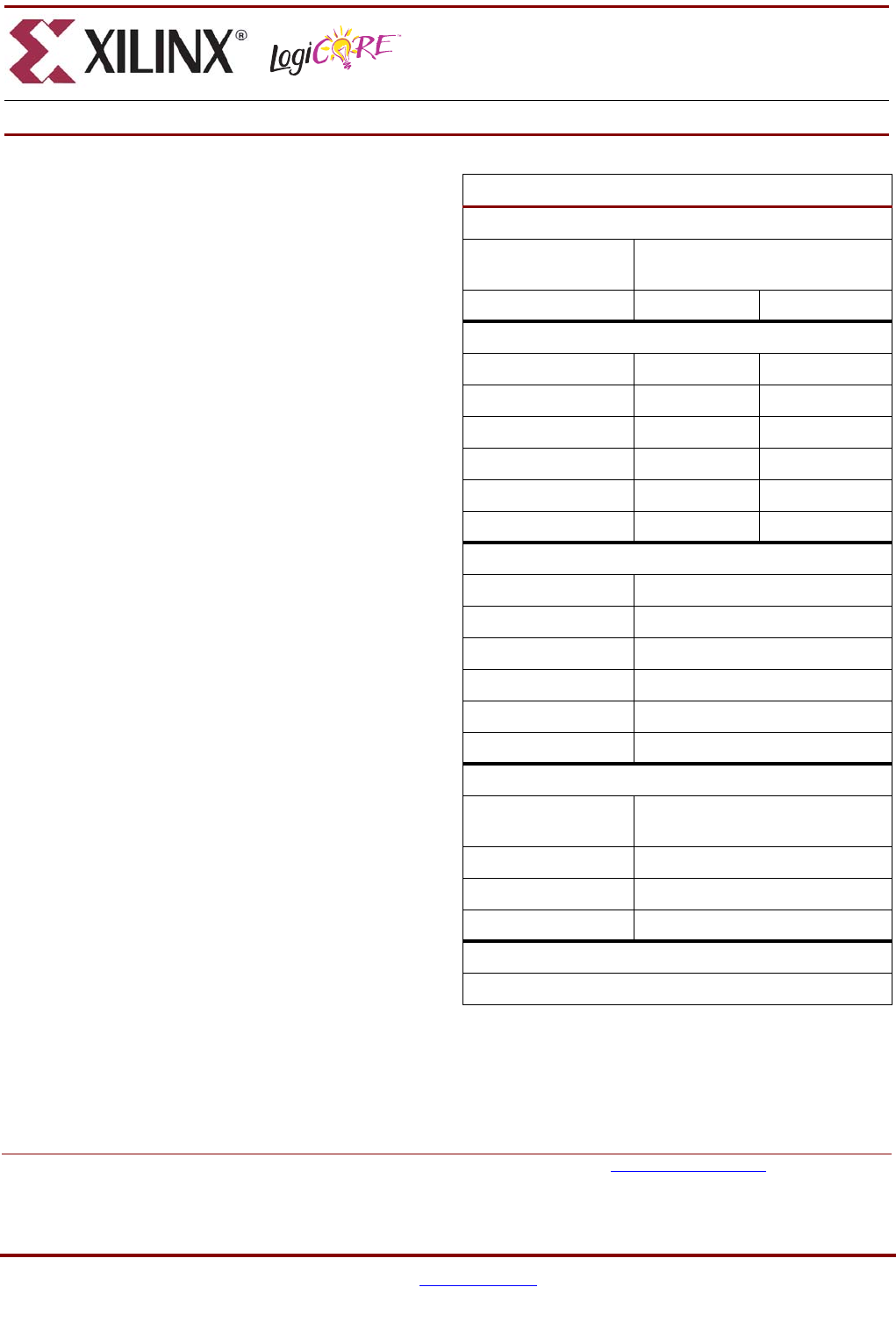
LogiCORE™ Facts
Core Specifics
Supported Device
Family
Virtex™-II Pro, Virtex-4
Version of Core plb_pci v1.00a
Resources Used
Virtex-IIP Min Max
I/O (PCI) 49 50
I/O (PLB-related) 397 433
LUTs 3350 3870
FFs 2570 2970
Block RAMs 8 8
Provided with Core
Documentation Product Specification
Design File Formats VHDL
Constraints File example UCF-file
Verification N/A
Instantiation Template N/A
Reference Designs None
Design Tool Requirements
Xilinx Implementation
Tools
8.1.1i or later
Verification N/A
Simulation ModelSim SE/EE 5.8d or later
Synthesis XST
Support
Support provided by Xilinx, Inc.