


PLB PCI Full Bridge (v1.00a)
14 www.xilinx.com DS508 March 21, 2006
Product Specification
EARLY ACCESS
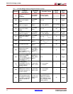
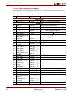
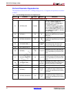
PLB PCI Bus Interface I/O Signals
The I/O signals for the PLB PCI Bridge are listed in Table 2. The interfaces referenced in this table are
shown in Figure 1 in the PLB PCI Bridge block diagram.
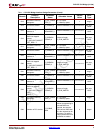
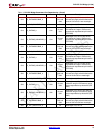
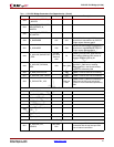
Table 2: PLB PCI Bridge I/O Signals
Port Signal Name Interface I/O Description
System Signals
P1 IP2INTC_Irpt Internal O Interrupt from IP to the Interrupt Controller
PLB Signals
P2 PLB_Clk PLB Bus I PLB main bus clock. See table note 1.
P3 PLB_Rst PLB Bus I PLB main bus reset. See table note 1.
P4
PLB_ABus(0:C_PLB_
AWIDTH-1)
PLB Bus I Note 1 applies from P4 to P53.
P5 PLB_PAValid PLB Bus I
P6
PLB_masterID(0:C_PLB
_MID_WIDTH-1)
PLB Bus I
P7 PLB_abort PLB Bus I
P8 PLB_RNW PLB Bus I
P9
PLB_BE(0:[C_PLB_DWI
DTH/8]-1)
PLB Bus I
P10 PLB_MSize(0:1) PLB Bus I
P11 PLB_size(0:3) PLB Bus I
P12 PLB_type(0:2) PLB Bus I
P13
PLB_wrDBus(0:C_PLB_
DWIDTH-1)
PLB Bus I
P14 PLB_wrBurst PLB Bus I
P15 PLB_rdBurst PLB Bus I
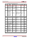
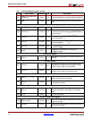
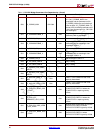
P16 Sl_addAck PLB Bus O
P17 Sl_SSize(0:1) PLB Bus O
P18 Sl_wait PLB Bus O
P19 Sl_rearbitrate PLB Bus O
P20 Sl_wrDAck PLB Bus O
P21 Sl_wrComp PLB Bus O
P22 Sl_wrBTerm PLB Bus O
P23
Sl_rdDBus(0:C_PLB_D
WIDTH-1)
PLB Bus O
P24 Sl_rdWdAddr(0:3) PLB Bus O
P25 Sl_rdDAck PLB Bus O
P26 Sl_rdComp PLB Bus O