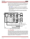
Read Datapath
R
Controller to Read Datapath Interface
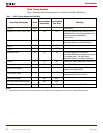
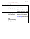
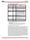
Table 4 lists the control signals between the controller and the read datapath.
Table 4: Signals between Controller and Read Datapath
Signal Name
Signal
Width
Signal Description Notes
ctrl_Dummyread_Start 1 Output from the controller to the
read datapath. When this signal
is asserted, the strobe and data
calibration begin.
This signal must be asserted when valid read data
is available on the data bus.
This signal is deasserted when the
dp_dly_slct_done signal is asserted.
dp_dly_slct_done 1 Output from the read datapath
to the controller indicating the
strobe and data calibration are
complete.
This signal is asserted when the data and strobe
have been calibrated.
Normal operation begins after this signal is
asserted.
ctrl_RdEn_div0 1 Output from the controller to the
read datapath used as the write
enable to the read data capture
FIFOs.
This signal is asserted for one CLKdiv_0 clock
cycle for a burst length of 4 and two clock cycles for
a burst length of 8.
The CAS latency and additive latency values
determine the timing relationship of this signal with
the read state.
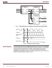
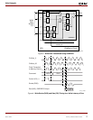
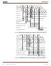
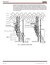
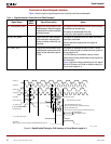
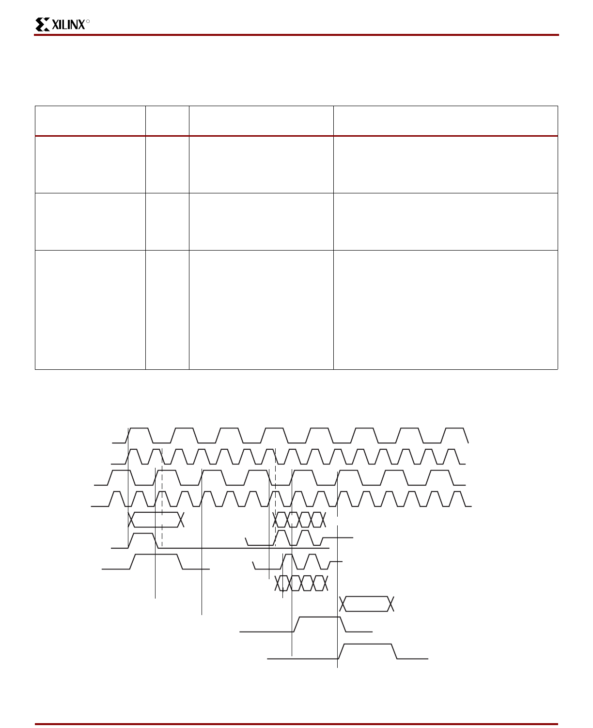
Figure 9 shows the timing waveform for this signal
with a CAS latency of 5 and an additive latency of
0 for a burst length of 4.
Figure 9: Read-Enable Timing for CAS Latency of 5 and Burst Length of 4
CLKdiv_0
CLKdiv_90
CLKfast_90
Command
CS# @ Memory
ctrl_RdEn_div0
srl_out (SRL16 Output)
Ctrl_RdEn
(Write_enable to FIFOs Aligned with ISERDES Data Output)
CLKfast_0
Parallel Data
@ ISERDES Output
DQ @ ISERDES Input
(Round Trip & Initial Tap Value & Calibration Delays)
DQS @ ISERDES CLK Input
(Round Trip & BUFIO & Calibration Delays)
D0,D1,D2,D3
X721_09_113005
D0
READ
D1 D2 D3
D0 D1 D2 D3
DQ @ Memory Device
DQS @ Memory Device
(Input to SRL16 Clocked
by CLKdiv_90)
64 Memory Interfaces Solution Guide March 2006


