Reference Design Utilization
R
Reference
Design
Utilization
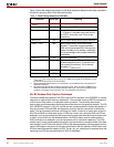
Table 5 lists the resource utilization for a 64-bit interface including the physical layer, the
controller, the user interface, and a synthesizable test bench.
Conclusion The data capture technique explained in this application note using ISERDES provides a good
margin for high-performance memory interfaces. The high margin can be achieved because all
the logic in the FPGA fabric is clocked at half the frequency of the interface, eliminating critical
paths.
Revision
History
The following table shows the revision history for this document.
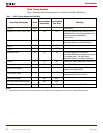
Table 5: Resource Utilization for a 64-Bit Interface
Resources Utilization Notes
Slices 5861 Includes the controller, synthesizable test bench, and the user
interface.
BUFGs 6 Includes one BUFG for the 200 MHz reference clock for the
IDELAY block.
BUFIOs 8 Equals the number of strobes in the interface.
DCMs 1
PMCDs 2
ISERDES 64 Equals the number of data bits in the interface.
OSERDES 88 Equals the sum of the data bits, strobes, and data mask bits.
Date Version Revision
12/15/05 1.0 Initial Xilinx release.
12/20/05 1.1 Updated Table 1.
01/04/06 1.2 Updated link to reference design file.
02/02/06 1.3 Updated Table 4.
66 Memory Interfaces Solution Guide March 2006


